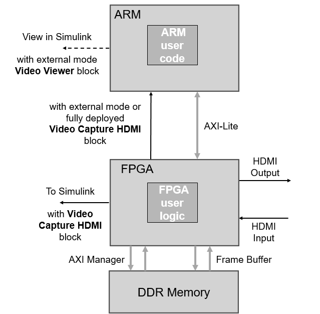
Zynq Video Dataflow for HDMI Input
SoC Blockset™ Support Package for AMD FPGA and SoC Devices assists you in targeting designs to the FPGA and ARM® processor on the Zynq® board. This page explains data path options for moving the video data between the FPGA, external memory, the ARM processor, and the Simulink® host computer, when your Zynq board is connected to a HDMI FMC card.
The video data input from the HDMI FMC module flows through the FPGA, including your customized FPGA user logic. The FPGA user logic can include an AXI-Stream interface to a frame buffer in external memory or an AXI manager interface for random memory access. The output of the FPGA is then sent back to the HDMI output. You can optionally export the video data to Simulink, or route it to the ARM processor. The video data is in streaming pixel format on the FPGA. When you import this video data to the ARM processor or Simulink, it is converted to frames.

Capture to Simulink
To capture frames to Simulink from the FPGA, use the Video Capture HDMI block. Get started by selecting one of these models that include the Video Capture HDMI block:
Template model for frame-based design. See Design Frame-Based Algorithms.
Template model for pixel streaming. See Design Pixel-Streaming Algorithms for Hardware Targeting.
Generated hardware interface model from HDL Workflow Advisor. This model also includes a Host AXI Interface block, with ports to read and write the AXI-Lite registers on the FPGA. See Models Generated from FPGA Targeting.
External Memory Interfaces
Template designs provide a simplified external memory interface model for simulation. For deployment, map this interface to the provided memory interface of the reference design. When you use an HDMI FMC card, you can model and deploy two kinds of external memory interfaces.
Frame Buffer –– The frame buffer interface stores an entire frame and returns the frame when requested. It recreates the streaming video control signals on the output frame. The reference design implements the frame buffer interface using AXI Video DMA.
AXI Manager –– The AXI manager interface provides read and write access to any address. It does not maintain streaming video control signals.
Capture to ARM Processor
To route video to the ARM processor, use the Video Capture HDMI block. You can run this block in external mode or and fully deploy it to the ARM processor. Get started by selecting one of these models:
New model. When you generate code for the ARM processor, it runs alongside the default FPGA image loaded at set up. You can change the video format of the captured data using the parameters on the Video Capture HDMI block.
Generated software interface model from HDL Workflow Advisor, after you load your custom FPGA logic to the board. This model already includes the Video Capture HDMI block. The pixel format parameters match the video format settings on the FPGA, and are informational only. This model also includes a Xilinx Zynq AXI Interface block, with ports to read and write the AXI-Lite registers on the FPGA. See Models Generated from FPGA Targeting.
In either of these models, you can view the modified video frames in Simulink by running the Video Viewer block in external mode.