Intel Agilex FPGA-in-the-Loop Simulation: Enabling DSP Emulation for Space-BACN
Ziyi Zhu, Intel
The U.S. Defense Advanced Research Projects Agency (DARPA) Space-Based Adaptive Communications Node (Space-BACN) program will provide communication in hard-to-reach areas by using a network of small low-Earth orbit satellites as relay stations to forward and amplify signals from ground-based radios, aircraft, and other communication systems, essentially acting as a space-based repeater system to extend the range of communication systems that would be limited by the curvature of the earth or interference from terrain. In the development phase, DARPA has selected Intel, with others, to design a reconfigurable optical modem that will support both current and new communication standards and protocols to enable interoperability among satellite constellations. Intel is developing its optical modem solution by bringing together experts from its field-programmable gate array (FPGA) product group, packaging technologists from its Assembly Test Technology Development (ATTD) division, and researchers from Intel Labs. Based on its leading-edge low-power Intel® Agilex™ FPGA, Intel is designing new chiplets that will be integrated using Intel’s embedded multi-die interconnect bridge (EMIB) and advanced interface bus (AIB) packaging technologies, into a single multi-chip package (MCP). To ensure first silicon success, Intel is using FPGA-in-the-loop technologies in MATLAB® and Simulink®. This enables the verification of HDL implementations directly against algorithms in MATLAB or Simulink, the application of data and test scenarios from MATLAB or Simulink to the HDL design on the FPGA, and the integration of existing HDL code with models under development in MATLAB or Simulink. Once completed, Space-BACN will be used in the future for humanitarian assistance, disaster relief, and operations in denied areas. Communication barriers that have long hindered operations in difficult environments will be overcome, allowing for greater efficiency and connectivity.
Published: 8 May 2023
[AUDIO LOGO]
Welcome to this presentation about Intel Agilex 7 FPGA-in-the-Loop Simulation. My name is Ziyi. In this talk, we will present the architecture, implementation, and results of FPGA-in-the-Loop Simulation on Intel Agilex 7 FPGA I-Series Development Kits. This technology enables Digital Signal Processing or DSP emulation for the DARPA Space-BACN Program. Our work is in collaboration with MathWorks and supported in part by the DARPA STO Office.
Here is the outline. This presentation will provide an overview of the DARPA's Space-BACN Program, including a discussion of the second technical area or TA2 system performance requirements and DSP building block considerations. We will discuss the challenges associated with DSP Emulation in pure software and how FPGA-in-the-Loop and Intel Agilex 7 FPGA I-Series can provide solutions.
Two FPGA-in-the-Loop architectures will be presented-- one using a Hard Processor System or HPS through ethernet connections and the other using PCI-Express links. Finally, we will demonstrate an FPGA-in-the-Loop simulation example design that accelerates a LTE Turbo Decoder using the Intel Agilex 7 FPGA I-Series Transceiver SOC Development Kit.
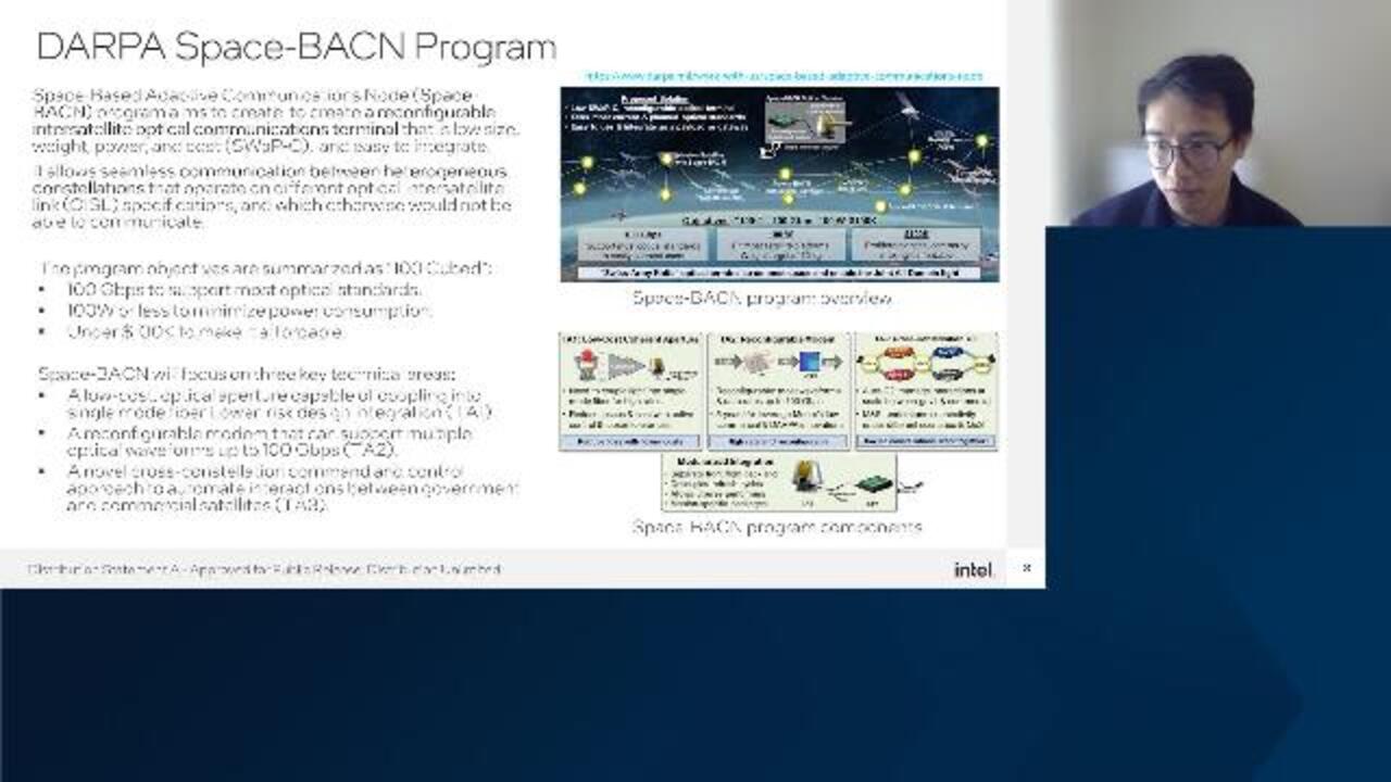
The Defense Advanced Research Project Agency or DARPA is developing a space-based communication node called Space-BACN. As shown in the program overview figure on the top right, the goal is to create a reconfigurable multi-protocol inter-satellite optical communications terminal that is low in size, weight, power, and cost. This terminal will be easy to integrate and will have the ability to connect heterogeneous constellations that operate on different optical inter-satellite link specifications.
The Space-BACN optical terminal aims to support all common optical waveforms up to 100 gigabits per second while using less than 100 watts of power and costing under $100K. These goals are known as 100 Cubed.
As shown in the program components figure, the Space-BACN Program consists of three technical areas. TA1 focuses on developing a low-cost, coherent optical aperture that couples light into a single mode fiber with high efficiency to support signal processing. TA2 focuses on developing a reconfigurable modem that can support multiple optical waveforms up to 100 gigabits per second and different DSP functionalities. TA3 focuses on developing a novel cross-constellation C2 approach that automates interactions between heterogeneous satellites.
The terminal is designed to be modular with interchangeable front and back ends. This allows for mission specific customization and component replacement in the future. Intel and other team members are working on the TA2 reconfigurable integrated modem. The work will comply with current optical inter-satellite link specifications and support the reconfigurability in modulation formats and coding schemes.
Here, we show the specifications. In TA2, performers are aiming to achieve the matrix specified for each program phase as outlined in the table located to the right. We will pause 30 seconds here for you to look at it. For more detailed information, please refer to the links provided below the table.
To meet the requirements, DSP blocks are necessary. And the designs must be verified. These include various modulation/demodulation formats, datarates, timing recovery loops, and Forward Error Correction or FEC encoder/decoders. The implementation considerations are shown on the left. Prior to fabricating the DSP chips that meet the TA2 requirements, it is necessary to implement these functional blocks in Hardware Description Language or HDL and verify their functionalities in simulation.
MathWorks, MATLAB, and Simulink software can be used for designing those DSP modules and verifying their functionalities. However, there are two challenges when designing and simulating impure software. First, it is unsure that the HDL implementation on the hardware will match the algorithms specifications. Second, simulation in pure software can be very time consuming. For instance, processing over 16 billion samples in the Turbo Decoder example can take days or even weeks in Simulink. We will show this design in later slides.
To address these challenges, we can use FPGA-in-the-Loop or FIL to achieve hardware AP verification and simulation acceleration on Intel [? FPGAs. ?] The FIL established a communication channel with the Design Under Test or DUT on the FPGA allowing for the transmission of input data and reception of output data in either the Simulink or MATLAB environment. FIL provides a verification and validation necessary for a full model-based design workflow. Detailed communication and processing architectures will be presented in later slides.
Intel Agilex 7 FPGA product family delivers on average 50% higher fabric performance and up to 40% lower total power consumption compared to previous generation Intel FPGAs. So Intel Agilex 7 FPGA I-Series is specifically designed for high performance processor interfaces and bandwidth intensive applications. So 0 to 7 product use in the development kit features hardened PCI Express Gen 5 support, integrated Hard Arm Processor, [INAUDIBLE] interfaces and 2.7 million Logic elements. These development kits are ideal to prototype and enable Intel Agilex 7 FPGA-in-the-Loop simulation.
This slide shows the data flow for the Ethernet FPGA-in-the-Loop architecture on the Intel Agilex 7 FPGA I-Series Transceiver SOC Development Kit. The data flow works as follows. First, my MATLAB transmits the input data over TCP/IP ethernet to a leap I/O daemon running in Linux on the Agilex HPS. The Leap I/O daemon interfaces with an [? I/O ?] kernel module to transfer the data into a kernel space buffer for Direct Memory Access or DMA reading.
Next, the memory mapped to streaming or MM to SDMA and the FPGA reads the data through the FPGA to HPS bridge and streams the data to the IFL interface wrapper. The data flows through the DUT and then out through the FIL interface to the streaming to memory map or S2MMDMA. The S2MMDMA then writes the data through the FPGA to HPS bridge into a kernel space buffer allocated by the I/O kernel module.
Finally, the Leap I/O daemon reads the buffer from the kernel module and then transfers the data back to MATLAB over TCP/IP Ethernet. The output data from the FIL is stored in a MATLAB workspace variable or displayed in Simulink. The Intel Agilex 7 FPGA I-Series Transceiver SOC Development Kit is shown on the right. Further information about the Agilex-associated Linux software build, LibIO and I/O kernel module can be found in the links below.
This slide shows the data flow for the PCI-E FPGA-in-the-Loop architecture on the Intel Agilex 7 FPGA I-Series Development Kit. The data flows works as follows. First, MATLAB transmits the input data to on chip or on board DR4 memory over PCI-E using the multi-channel DMA kernel driver and the multi-channel DMA IP.
Next, the MM2SDMA on the FPGA reads and streams the data to the FIL interface wrapper. The data flows through the DUT and then out through the FIL interface to the S2MMDMA. The S2MMDMA then writes the output data to on chip or on board data for memory.
Finally, MATLAB retrieves the data over PCI-E using the multichannel DMA Kernel driver and the multichannel DMA IP. The output data from the FIL is stored in a MATLAB workspace variable or displayed in Simulink. Please note the multichannel DMA IP has streaming ports. And they can be enabled to bypass on-chip or on-board [? DR4 ?] memory-- MM2S and S2MMDMAs.
Both data flows are planned to be supported. The Intel Agilex 7 FPGA I-Series Development Kit is shown on the right. Further information about the multichannel DMA for PCI-Express IP and design example user guides can be found in the links below.
Here, we demonstrate the use of FPGA-in-the-Loop simulation for both verification and hardware acceleration of an LTE Turbo Decoder example design. The DUT is a LTE Turbo Decoder block highlighted in right from the wireless HTL toolbox. This block provides an interface and architecture that is optimized for HTL code generation and hardware implementation on the Intel Agilex 7 FPGA. The block uses a fixed point data type resulting in different bit error rate or BER performance compared to the floating point LTE Turbo Decode function in MATLAB. As such, it is necessary to characterize the hardware performance by matching the BER over a range of signal-to-noise ratio or SNR values and comparing it to the floating point result in the software.
To make the BER measurements, this demo consists of three stages. Data generation, DUT execution, and verification. First, transmitted frames are randomly generated and then converted into an encoded QPSK format using the LTE Turbo Encode and LTE sample modulate functions. Based on different SNR values. Additive white Gaussian noise is applied to the I and Q channels to simulate the received noisy data. The LTE symbol demodulate function is then used to convert the QPSK data back into bit frames before being input into the DUT.
Both the floating point function in MATLAB and the fixed point hardware implementation through FPGA-in-the-Loop are executed. Finally, BER measurements are performed on both outputs for the verification. There are two modes in this FPGA in the Loop simulation example.
First, cycle [INAUDIBLE] mode. In this mode, the LTE Turbo Decoder DUT is triggered cycle by cycle from the MATLAB or Simulink environment. It requires padding data to trigger the clock and achieves the cycle accurate verification of the DUT. Second, free running mode.
In this mode, the DUT receives both input samples and ground [? truth ?] bits. After all the samples are processed and the [INAUDIBLE] are counted on the FPGA, the BER results are retrieved back to the MATLAB or Simulink environment. For further information regarding the LTE Turbo Encoder and Decoder, please refer to the links provided on this slide.
This slide presents the result. The left figure shows the bit and cycle accuracy between the hardware LTE Turbo Decoder and the source Simulink model used to generate the HTL code. The decoded bits match precisely between the fixed point reference implementation and the actual bits calculated on the FPGA. The arrow curve remains at 0. The EB over and all or Eb/N0 represents the energy per bit, the noise power spectral density ratio.
The red figure shows the BER measurements of 1 billion samples per Eb/N0 value. We observed a large acceleration of FPGA-in-the-Loop Simulation with free running mode for simulating the LTE Turbo Decoder. With FIL free running mode, it took around 23 minutes to simulate 1 billion bits for 16 Eb/N0 values. In contrast, it would take approximately 21.5 days for simulation in pure software and approximately two days for the FPGA-in-the-Loop Simulation with cycle accurate mode.
The small BER performance degradation of the FPGA-in-the-Loop is due to floating point to fixed point conversion. The experimental results were obtained using MathWorks server machines and Intel Agilex 7 FPGA I-Series Transceiver associated development kit. We will be able to accelerate the emulation process of the Space-BACN blocks by using the FPGA-in-the-Loop Simulation. This is the end of my talk. Thank you for your attention.
[AUDIO LOGO]
Related Products
Learn More
Featured Product
MATLAB
Up Next:

Related Videos:


Select a Web Site
Choose a web site to get translated content where available and see local events and offers. Based on your location, we recommend that you select: United States.
You can also select a web site from the following list
Americas
- América Latina (Español)
- Canada (English)
- United States (English)
Europe
- Belgium (English)
- Denmark (English)
- Deutschland (Deutsch)
- España (Español)
- Finland (English)
- France (Français)
- Ireland (English)
- Italia (Italiano)
- Luxembourg (English)
- Netherlands (English)
- Norway (English)
- Österreich (Deutsch)
- Portugal (English)
- Sweden (English)
- Switzerland
- United Kingdom (English)