Loop Gain Calculation for Current-Programmed Mode Control of Switched-Mode Power Supplies
You can derive a small-signal model of the current-programmed mode (CPM) control loop with power train and pulse width modulator (PWM). You can then use the small-signal model to study the pole locations for the control loop, the loop’s Bode plot, and the time domain simulated step response as a function of loop gain.
CPM has been known since 1978 and has been widely used in the power supply industry since then. Here, you can see a simplified control loop analysis by basing the analysis on the sensed current at the falling edge of the power train control signal rather than the average sensed current. For more information on CPM, see [1].
To perform the simplified control loop analysis, follow these steps:
Perform a power train operating point analysis in which the falling edge is at the start of the switching cycle, producing a small-signal control model of the power train.
Create a small-signal linear model of the pulse width modulator (PWM) based on the derivatives of the sensed current and artificial ramp at the falling edge of the control signal. The inputs to this model are the PWM control signal and the power train continuous time state of the power train.
Replace the duty cycle input to the power train small signal model with the linear expression containing the PWM control signal and the power train state.
Examine the impact of this transformation on the A matrix of the power train control model.
You can apply this method to the operating point analysis of a buck power train and demonstrate the time-domain simulation results for several choices of CPM loop gain.
Small-Signal Model
Consider an operating point analysis of a power train is performed in which the falling edge of the control signal is at the beginning of the switching cycle. The additional underlying assumptions are:
fixed-frequency PWM,
operating point controlled by duty cycle through direct control of the PWM, and
direct sensing of inductor current.
The small-signal model produced by this analysis can be partitioned into the form:
where is the vector of input variations, is the duty cycle variation, is the vector of output variations, and is specifically the variation of the sensed current. Note that by definition the duty cycle does not feed directly through to the output, so the corresponding entries in the D matrix are zero.
The equivalent block diagram of the PWM circuit is shown:

It includes an artificial ramp generator, an amplifier for the sensed current, and a comparator to compare the input control voltage to the sum of the ramp and the sensed current. The falling edge of the control signal occurs when:
Shifting the control voltage Vc by a small increment and Vsns waveform by produces a small increment τ in the time at which the latch reset occurs, such that:
Assuming the slope of the current sense voltage at the falling edge is mvsns and the slope of the ramp voltage is mva:
Subtracting the steady state values out:
Given clock period Ts, the change to the duty cycle is:
The inductor current is a direct element of the circuit state, and so assuming that Vsns is an accurate measurement of the inductor current with minimal interference from the power train input, Dss2 is zero. The output equation of the small signal model then produces:
Finally, plugging this result back into the state equation:
Note in this equation that the CPM loop directly modifies the A matrix of the small signal model and therefore its poles. In other words, CPM acts as instantaneous feedback on the small signal state rather than as a slower external compensator. You can use this modified A matrix to study how the gain G of the CPM loop modifies the poles to be managed by an outer voltage control loop.
Operating Point Analysis
You can use the operating point analysis of a buck converter power train circuit to explore the effect of CPM loop gain on the poles of the small signal model.

Perform an operating point analysis to get its output as a function of duty cycle. Note
in this operating point analysis that the phase offsets should be set to
1-d rather than 0 to start the control signal at the
falling edge rather than the rising edge that is more typically used.

In addition to the calculation of the output as a function of duty cycle, the operating
point analysis produces an abcd struct containing the A,B,C,D matrices
for a small signal model of the power train at the operating point, as well as a table of
waveforms for every voltage and current node in the circuit. Use the A,B,C,D matrices for
subsequent direct manipulation to determine the effect of CPM.
Use the waves output to access the table of steady state switching
cycle waveforms and get parameters specific to the CPM analysis. You can obtain slope
mvsns from the minimum and maximum current
sense voltage, the duty cycle D, and the clock period:
Assuming a one volt artificial ramp:
And the maximum stable gain is:
You can then quickly calculate the poles for a wide variety of gain values by calculating the closed loop A matrix and then taking the roots of .
| G | Poles (1) | Poles (2) |
|---|---|---|
0 | -895.21+6255.3i | -895.21-6255.3i |
1 | -3609.6+5476i | -3609.6-5476i |
2 | -6191+2760.9i | -6191-2760.9i |
2.25 | -6816.7+441.3i | -6816.7-441.3i |
2.3 | -8112.8 | -5769 |
3 | -13754 | -3544 |
5 | -24230 | -2226 |
10 | -44612 | -1459 |
31 | -97736 | -972 |
Note in these results that up to a gain of 2.25 the poles form a complex pole pair, with
the Q of the pole pair decreasing from a Q of 7
(consistent with [2]) for G = 0 to a
Q less than 1 (critically damped) for G =
2. Somewhere between 2.25 and 2.3, the pole pair splits into two
real-valued poles and the separation between these poles increases as the gain increases. A
lower Q or a set of split poles produces a response to load current steps that is smoother
and easier to control.
You can also create a Control System Toolbox™
ss object (state space model) that represents the CPM loop containing the
power train and then produce a Bode plot for that control loop, for example to assess how
difficult it will be to design a voltage-programmed mode control loop that contains the CPM
loop. A gain of 2 produces the following result:
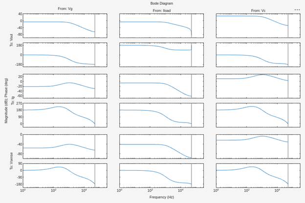
Note that the magnitude response from Vc to Vout is flat, and there is only a modest variation in the corresponding phase response. This power train should be very easy for an outer voltage loop to control.
Time-Domain Simulation
You can use a Simulink® model to evaluate the load step response of the CPM loop as a function of loop gain. This section compares the load step response for three design choices:
G =
0— Open loop.G =
(Gmax/2)— Commonly referred to as the deadbeat response.G =
2— Critically damped.
The Power Train block in the model uses the same buck power train that is used for the operating point analysis.
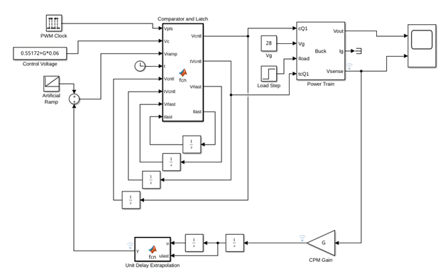
This model contains two MATLAB® function blocks. The Comparator and Latch block is designed to model the timing of the PWM comparator and latch as precisely as possible within a fixed step discrete Simulink model. The Unit Delay Extrapolation block is combined with two unit delay blocks to convince Simulink that the model contains a delay in the feedback loop while also providing the Comparator and Latch block with Vsense samples that closely approximate the Vsense output of the Power Train block at the same sample time.
In addition to producing the gate control voltage cQ1 for the Power Train, the Comparator and Latch block also provides the precise timing of the gate control transition through the tcQ1 signal. The output of the Comparator and Latch block is also fed back to its input for use in the next sample time.
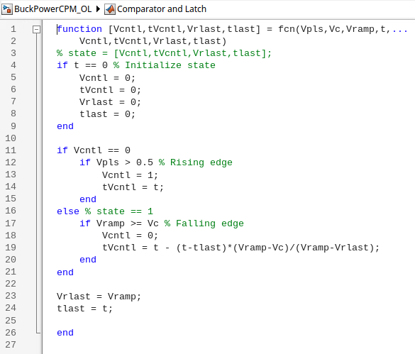
Line 19 in this code uses linear interpolation to determine the exact time when the comparator output will switch from zero to one.
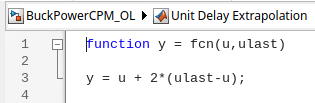
Line 3 extrapolates from the previous two samples to predict the current sample at the output of the CPM Gain block. This extrapolation is very accurate except for the sample that immediately follows a control signal transition. However since the transition has already occurred when that sample is produced, its value is irrelevant to the simulation
At T = 0.01, the Load Step block increases the
load current by 5 amps. Given that before that time the output current is the 15V output of
the power supply applied to the 3 ohm load resistor internal to the Power Train model, the
net result is to double the Power Train’s output current.
The open loop response (G = 0) is shown:
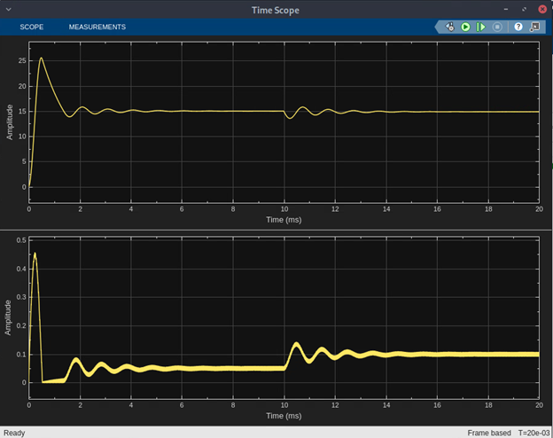
Note the large start-up transient and ringing, and the significant ringing at the load step. This is a direct result of the fact that the Q of the Power Train poles in this configuration is 7.
A commonly selected design point is to set the CPM gain to one half the maximum CPM gain, the so-called deadbeat response because the input to the comparator remains essentially constant after the falling edge of the control signal. The step response for this design choice is shown below:
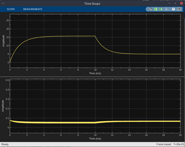
Note the absence of a startup transient and the very smooth load step response.
When the CPM loop is configured to be approximately critically damped
(G = 2), the response becomes:
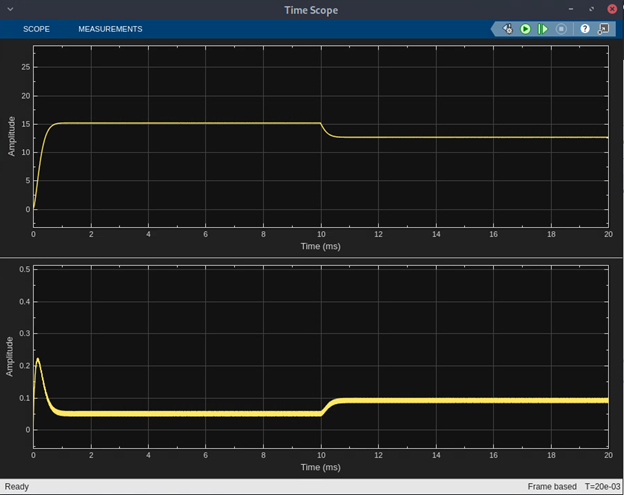
Note the relatively rapid response to the load step, with a total absence of ringing. This could be a very valuable characteristic, for example when driving a digital load that has rapid changes in current due to changes in operating conditions. Note also that while there is a start-up transient, it is not extreme and could be controlled with a start-up ramp in the control voltage Vc.
References
[1] Erickson, Robert W., and Dragan Maksimović. Fundamentals of Power Electronics. Third edition, Chapter 18. Springer, 2020.
[2] Basso, Christophe P. Designing Control Loops for Linear and Switching Power Supplies: A Tutorial Guide. Appendix 4a. Power Engineering. Artech House, 2012.