Optimization of Mixed-Signal ICs with MATLAB - MATLAB & Simulink
Video Player is loading.
Current Time 0:00
Duration 49:23
Loaded: 0.33%
Stream Type LIVE
Remaining Time 49:23
 
1x
  • Chapters
  • descriptions off, selected
  • captions off, selected
  • en (Main), selected
    Video length is 49:23

    Optimization of Mixed-Signal ICs with MATLAB

    Overview

    As analog mixed-signal integrated circuits (ICs) become increasingly complex, gaining deep insights and exploring innovative ideas is crucial for success. We will demonstrate how to combine MATLAB and Cadence Virtuoso to improve the design workflow and optimize the performance of your IC.

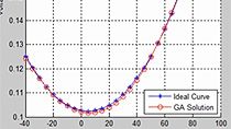
    Using practical examples, we will show how to take control of design variables and parameters in Cadence Virtuoso directly from MATLAB. Run simulations programmatically, analyze the design space, and use surrogate optimization methods to improve the performance of transistor-level IC designs.

    You will learn how to directly import waveforms and metrics from Cadence Virtuoso into MATLAB and leverage advanced analysis functions. Discover how to measure phase noise, identify poles and zeros, fit curves with various algorithms, and even apply your favorite MATLAB functions for in-depth analysis. Automation will be a key focus, as we showcase speeding up recurrent tasks, facilitating design space exploration, and generating comprehensive reports for seamless collaboration with your colleagues.

    Last, we will export models from Simulink using behavioral languages such as SystemVerilog and VerilogA for IC design and verification. Use MATLAB to rapidly develop digital signal processing algorithms to control and calibrate the impairments of your IC implementation and optimize the performance of your mixed-signal system.

    Highlights

    • Explore the IC design space and control Cadence simulation from MATLAB
    • Import waveforms and metrics from Cadence Virtuoso
    • Analyze trends and generate reports from IC simulation results
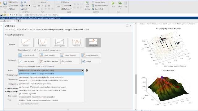
    • Optimize transistor-level design using surrogate optimization methods
    • Export SystemVerilog and VerilogA models from Simulink for IC integration and verification

    About the Presenter

    Giorgia Zucchelli is the product manager for RF and mixed-signal at MathWorks. Before moving to this role in 2012, she was an application engineer focusing on signal processing and communications systems and specializing in analog simulation. Before joining MathWorks in 2009, Giorgia worked at NXP Semiconductors on mixed-signal verification methodologies and at Philips Research developing system-level models for innovative telecommunication systems. Giorgia has a master’s degree in electronic engineering and a doctorate in electronics for telecommunications from the University of Bologna. Her thesis dealt with modeling high-frequency RF devices.

    Recorded: 17 Apr 2024

    Hello. Today we're going to talk about optimization of mixed-signal integrated circuits with MATLAB. My name is Giorgia Zucchelli. And I'm product manager for the RF and mixed-signal areas at MathWorks.

    The topic of today is a burning issue. And I receive a lot of questions about MATLAB and how can MATLAB help with the design and performance optimizations of mixed-signal ICs. So I thought to provide you with a set of tools that can better help you with achieving your goals.

    There is a lot of interest in mixed-signal optimization because the complexity of integrated circuits is exponentially increasing, driven by smaller integrated circuit size, increased level of functionality, faster speed, lower power, smaller processes with higher variability, tighter integration that requires a parasitic effect correction and calibration. And such complexity can barely be handled using traditional techniques.

    And this is where computer-aided design automation can help. And specifically, it can help designers by providing behavioral models that enable early verification with different optimization techniques, different statistical approaches for design experiments, and can help also with AI to solve particularly difficult problems or problems that are based on-- that require the analysis of a lot of data.

    So you can see how integrated circuit design can be helped by MATLAB, but that provides tools in each of these specific areas. Today, we are going to particularly talk about optimization and the use of behavioral models for early verification and improve the design.

    IC optimization can mean different things. And today, we're going to talk with two examples of IC optimization. We're going to talk about design optimization-- so the optimization that happens at the transistor level and that is done at the silicon design time. We will see, for example, how to scale the sizes of transistors, for example, to minimize layout parasitic effects, power consumptions, area, or speed.

    There is also another aspect related to optimization that is what I call performance optimization that happens much more at the architectural or algorithmic level. In this case, the optimization algorithm is actually executed at runtime or at calibration time together with the integrated circuit. So you can think of performance optimization when you have systems such as adaptive equalizers or a linearization algorithm or calibration circuits to compensate for PVT variation or even analog trimming.

    So these two optimizations are different. But they share some common problems. And in particular, if you are embarking in any of these optimization, you need to answer this question. What is the objective function? What is the ultimate goal that you want to achieve? What is the specific metric that you want to optimize? What are the variables that you can vary to achieve your goals?

    What are the bounds of these variables and the acceptable values? So you could say that if you don't provide a bounded problem, for example, you could end up with a capacitor that is the size of the sun. That's not particularly helpful.

    What are the additional constraints that you need to respect? For example, you might shrink the area of an IC. But you still need to achieve, for example, a certain gain or a certain bandwidth.

    And what is the best optimization algorithm that you can use? Do you need to take into account global or local optimization constraints, for example?

    So we are going to see two examples today. And we're going to start with the first example, where we design-- where we optimize the design of an operational amplifier.

    This is the circuit that we are-- we'll optimize-- is just less than a dozen of transistors. So it's relatively simple. And as part of-- and we want to use this example to provide a recipe on how to go about with more complex systems.

    So the first step consist in identifying the variable and the bounds and the valid values that we want to optimize. In this case, we have selected the sizes of the transistors-- so width, length, and multiplication factor. And as some of the transistor appeared in a mirror configuration, some of these variables are actually coupled.

    It's also interesting that, for example, the length of a transistor can only be changed by a fraction of a micrometer-- so 0.1 micrometers-- which means that it's not a continuous optimization. But effectively, it turns into an integer optimization.

    The second point or the second steps in our recipe consists in identifying the constraints. So what are the metrics? In this case, we have a bandwidth, current, gain, a slew rate, and a unity-gain bandwidth. These are metrics that are obtained as a result of transient AC and DC simulation on the circuit.

    We provide constraints we want-- for example, the bandwidth of-- the 3D bandwidth to be larger than 2 megahertz. But we also define a weight, which says how important is on a scale from 1 to 100 in meeting this specific constraint. And we use weight to combine the constraints and to allow us to say whether we met our target or not.

    The third step is based on a simple observation that if we would do a brute force analysis of this circuit by simply simulating all possible combinations of values for the different transistors, we would end up with having to simulate more than 10 million or billions of simulation of a 1.3 e16. This is not possible. It's just not a feasible brute force approach. So for this reason, instead of doing a brute force approach, we use a surrogate optimization method, a method that builds a surrogate model of our circuit to reduce the number of simulation and still find an optimum for the design.

    The fourth and the fifth step of our recipe are fairly straightforward. We run the simulation and we apply the results to our IC design. And you can repeat this operation iteratively-- for example, if you are exploring different constraints, different goals, or if you want to break down the problem into smaller issues.

    With this, let's see how this problem looks in practice. Let's open up our Cadence database and test bench for our op-amp and the Maestro view. This is our design. So let's take a look at it.

    We open our design. And we see that it has a couple of layers in the hierarchy. The top layer is, essentially, the op-amp and-- with these supply settings, supply and bias generation. We look one layer down. We see the schematic of the actual op-amp with transistor implementation.

    We open as an assistant the variables and parameters. And we can verify now how the different variables for the transistors are coupled. For example, we see that transistor 24 and 18 are-- use the same variables. So this is transistor 18. And you see here on the top that 18 use the same variables at 24 in this case, which is-- 27 and 25 use also the same variables. So match transistors, essentially, have matched design variables.

    And this is how we set up our problems. And this is the problem that we want to resolve. You see also here on the left-hand side in the panel the variables with the bounds and steps as we have defined.

    In the middle, we find the metrics. And the metrics are determined based on transient AC and DC simulation. You see that we define the bandwidth, the current, gain, and the relative specs with the constraints-- so for example, the gain has to be greater than 35 dB-- as well as the relative weight-- in this case, the weight of 100.

    So this is how we set up the problem in Cadence. And we can now run the simulation, the nominal simulation for the nominal value of the variables. And we, indeed, see that for both the gain and the slew rate that we don't meet our constraint.

    In the next 10 minutes or so, we are going to see how MATLAB can help us in automatically scaling the dimensions of the transistors in such a way that we can meet our constraints and our optimization objectives so that when we apply this computed width and length and multiplication factors, we actually meet all our specifications. But before diving into our optimization problem, let's take a small step back and let's look at our design parameters.

    If we enable them and ungroup the parametric set, if we perform a brute force sweep, we will have to run over 1 e16 simulations. This is not acceptable. But we still want to run a subset of the simulation to get a feeling for the sensitivity of our circuit. So what I'm going to do now is to disable each of the variables. And as I disable the variables, you will see the number of point sweeps decreasing. And you also see how the variables are coupled together. So when I disable one, the match transistor also gets disabled.

    And I'm going to perform just a sweep in two variables-- that is, the width and the length of transistor 24. And I'm going to increase the step over which I perform this sweep to 1 micrometer. And just sweeping two variables, I have to perform 304 simulations.

    I run the simulation. And I now get a new data set that is interactive one. You see here that I get all the 304 simulations. And what is interesting also is that we fail our target in all the simulations.

    So this already is useful information because it can give us some idea about the sensitivity of the circuit. So let's analyze this data. And let's analyze it in MATLAB. So I'm going to invoke MATLAB directly from the Maestro view.

    And as MATLAB opens up and loads in the background, what we find in our workspace is an object that is called adeinfo. This provides a link to our Cadence setup and our project and our simulation results.

    We could operate directly on the adeinfo. But instead, we use the mixed-signal analyzer app to directly import the data. So I import the interactive 1 run-- so with 304 simulations. And we'll get the data directly accessible from MATLAB for me to visualize and to inspect.

    So I see here the data gets loaded. I select the gain. And I'm going to plot it over a trend chart. So we're going to want to see the trend of the gain over the length and width of transistor 24. So in this case, we are going to put the width over the x-axis and the length over the legend. We can have multiple categorical axes with this view. And we can see how, essentially, the gain has a fairly smooth trend over width and length-- well, there is a different trade-off that provides the maximum gain.

    What is also interesting and useful here is that we can cross-probe the curves and the data set-- so to identify specific data points. In a similar way, I can plot a slew rate-- that was the other metric that didn't meet our target-- and, again, have a plot-- a trend chart with a similar plotting and, again, verify a slightly-- the behavior, which is, in this case, slightly different and slightly less predictable.

    We can also compare these two behaviors next to each other and, eyeballing, try to find a trade-off between the two behavior that allows us to meet the desired specification. But of course, as the design space becomes larger as the number of constraints increases, it becomes harder and harder to perform this operation manually. But this provides some help in understanding your enemy.

    So before we start with the optimization, an operation that we have performed is understanding the sensitivity of our integrated circuit. We do this by exploring a limited subset of configurations for our design variables. And we used MATLAB to analyze and identify major trends. This helps us in understanding what is the metric that matters, but also what is the metric sensitive to-- in other words, if I change the size of a transistor or the length or which transistors impact most the performance.

    This is a very common operation that any designer needs to perform while designing a system because it provides insights and understanding on how the overall performance works. But again, we can't use this approach to optimize our circuit because the number of simulations that would be required is-- are just unfeasible. But it's a good learning point that provides-- that helps the designer providing guidance to the optimization algorithm itself.

    So let's now go to our first step in the recipe and import the variables, as we have defined them in the Cadence Virtuoso setup. We are going to read, identify the independent variables. We are going to identify the bounds and figure out if only discrete values are allowed. Then we need to set up the optimization algorithm in such a way that it can perform an integer optimization.

    So here we use a couple of helper functions where, essentially, we use the adeinfo object to read what are the independent variables and, essentially, make them available in MATLAB as a lookup table. So you see, for example, that for the first variable, we find out what is the name, what is the lower bound, the upper bound, but also, importantly, what is the scale factor-- in other words, what makes the sweeping of the variable into a-- on an integer set.

    So let's see our first step in the optimization directly from MATLAB. Here I open up a script that is based on a shipping example that you can find in the mixed-signal block set. The first line of the script consists in interrogating the adeinfo object to extract the output table.

    The output table provides the list of metrics, constraints, and weights as we have defined them in Cadence. We simply read the data and make it accessible in MATLAB as a table on which we can operate. So you see here all the information.

    And in the script, we also interrogate the adeinfo object to identify the variable names, the scale factor, the lower bound, and the upper bounds. And we, again, put the variables into a parametric table. This is, again, the same information that we had in Cadence. But now it's accessible in MATLAB. And we can use this information as a basis for our optimization.

    Notice that all these functions that we see here in the MATLAB script are helper functions that are open. And you can inspect them as defined as part of the shipping example. Again, we can verify that the variables and the metrics are the same that we also defined in our Maestro view.

    The second step in our optimization problem consists in identifying the scales constraints. So in Cadence Virtuoso, we have defined our set of constraints, like bandwidth, current, gain, and slew rate, whether to be greater than or smaller than a certain threshold. But what is interesting to observe is that each of these metrics-- they have a different unit and a different scale. So for example, we go from a current that is in the order of microamperes to a bandwidth that is in the range of megahertz-- so 1, 6-- to a gain that is in the range of dB.

    So we have constraints that have very different ranges. When the optimization is performed, we need to determine how close we are to our goal. And for this reason, we need to scale the constraints so that they can be combined into a single metric.

    In other word, we need to build a single cost function where the constraints are suitably combined through a factor that is a function of the value of the constraint and is relative weight. In this case, for example, we will need to combine very large properties, such as the bandwidth, with very small properties, such as the current, with something that is somewhat in between, such as the gain.

    Additionally, we need to turn all maximization targets into a minimization problem. This is because often, optimization algorithm are looking for the minimum of the cost function. And to do this, we apply an inequality sign. So instead of maximizing the gain, we will try to minimize the negative of the gain.

    So we go back to our MATLAB script. And we extract the constraints from the output table. The constraints only consist of the metrics, the threshold, and the specification plus the weight. If we use this information to identify what is our objective function, in this case, we simply use the gain because it's the constraint with the maximum weight. And we also define the scale constraint by normalizing the value of each of these metric by its target threshold and then multiplying it times the weight.

    As a third step in our recipe for IC design optimization, we set up the configuration for our optimization algorithm. And this optimization algorithm lives in MATLAB and, in particular, in the Global Optimization Toolbox.

    First of all, we need to say what is the objective function. What is the cost function that we want to minimize? So in this case, we identify the gain. And then we also, additionally, include the scaled constraints to determine our cost function.

    Again, we use a helper function here that is called getMetrics. And we use a function handle so that we can pass the handle-- or the pointer to this function to our optimization algorithm so that it can sweep the design variables and recompute the cost function while it iterates throughout the optimization process.

    Next, we choose a specific optimization algorithm. We use the surrogate optimization algorithm. It's a global optimization algorithm with very robust properties for non-continuous problem, but also very fast to evaluate the expensive cost functions. And we tell the surrogate optimization method to run eight parallel simulation at the time. In this way, the surrogate model is built more rapidly.

    We additionally include a custom plot function to visualize progress to have, while the simulation is running, a feeling for how close or far we are from our desired objective. And we also include a checkpoint file that can be used to save and restart the optimization.

    So say that I run, I don't know, 60 optimization simulations, 60 simulations and I still do not converge. I can tweak some of the parameters and restart from where I left last time. In that way, I have better control of where we are with the optimization algorithm.

    Let's now go back to our script and see how the optimization problem was set up. First, we need to define the objective function. And this is really important. The function getMetrics is structured as follows. The first input, x, actually are the variables over which we want to optimize the circuit. These are the 10 independent variables that define the transistors' sizes.

    The second variable is the goalName, which, in our case, is gain. The third variables are the variable names-- so the variables that we want to optimize in our circuit-- the scale factors, and the constraints table.

    The function getMetrics is actually a custom function that we just defined for the specific optimization. You can open it, inspect it, and, if you like, modify it to your own specific problem.

    So now we understand the objective function. Let's see the other parameters for the optimizer. We will decide to run eight parallel simulation in Cadence for a maximum of 32 simulations. This could be a much larger number. We also have a custom plot function. And one last parameter that is interesting is the variable intcon that is defined here at line 18.

    This simply says that all the variables in our optimization are actually integer variable. In other words, the surrogate optimization method can solve a mixed-integer problem. Everything gets bundled together into a single object that we will call options that we will pass directly to the optimizer.

    The fourth step in our recipe for IC design optimization consists in, very simply, running the optimizer. So we run the optimizer directly from MATLAB. So we invoke our surrogate optimization method, passing the objective function as a handle, the lower bounds, the upper bounds for our design variables. And we also specify that this is an integer-- the variables of-- are only allowed to take integer values.

    As we run the simulation, as we run the optimizer, we will see the simulations in Cadence running in the background. We see the simulation being populated. And we can also see the progress of our-- in our custom plot function on how close we get to the final solution until, actually, we converge to the-- we meet the objective in only three iterations.

    Back to our script, let's run the optimization. In this case, we will not use a checkpoint file. We will simply run the surrogate optimization method, passing our objective function, getMetrics, the lower bounds for the design variable, the upper bounds, the array of integer that indicates which variables are integer for a mixed-integer problem, and, of course, the options.

    As the optimization starts, we see in Cadence the progress. We run eight simulation at the time. You see the pie getting fuller. You see the results getting ready. And we go through multiple sets. And so every new simulation set gets new initial values for the optimizer to run and to build the surrogate model.

    As the optimization converges, the simulation completes. And we can see that here towards the end, one of the last iterations meets all our constraints and our target gain. We can also see that in our custom plot function at iteration 23, we achieved a gain of 36 dB.

    So we can now go back to MATLAB and actually extract the final metrics. So we can see, for example, that now the gain is greater than 35 dB. And the slew rate meets the specifications as well as the value of the variables that allowed us to achieve this result.

    As the last step in our recipe for IC design optimization, we apply the results. We run the simulation in Cadence. And we need to verify that we met our target and that the design performs as we desire. And this is the point where you can further elaborate your design.

    Back to our MATLAB script for our last command, setFinalSolution-- we apply the exact values of the variables that were returned by the optimizer to our design. And we rerun the simulation simply to verify that these values provide, indeed, the desired outcome. And as we can see, we meet all our targets. We have all passes. And we are successful in our attempt of optimizing the design.

    Let's now cover some of the techniques that we used to perform our task and, in particular, how MATLAB helped with data analysis, identifying trends, and how MATLAB works as a controller of the Cadence simulation. What we've used a lot is Cadence. We've done lots of simulations in Cadence Virtuoso. And we invoked-- we use the M button to directly pass the results of the simulations into MATLAB.

    By invoking the M button from the Cadence Virtuoso-- Cadence Maestro view, what we end up is with a variable, adeinfo, in the MATLAB workspace. And this adeinfo provides a pointer to the entire Cadence project as well as simulation results.

    From here, for example, we can visualize the results and identify trends. So we have seen how to plot the different metrics. And you can really use the entire power of MATLAB within the mixed-signal analyzer app to take advantage of all analysis function, all regressions, all fitting, all sort of analytical tools, as well as ability to generate reports, to further understand the behavior of your integrated circuit.

    We've also taken this workflow one step further. So from Cadence, again, we invoke the M button. We created our adeinfo object in the MATLAB workspace. But we use this adeinfo object to probe all the parameters of our designs. And this can be parameters or variables, essentially, using the command adeGet. By just simply invoking the adeGet, you find all the variables that you have defined in your design space in Cadence. And you can visualize what are the variables and what are the bounds, as well as the step, on which we can vary the variables.

    So we went from Cadence to adeinfo. And then we use adeGet. From here, we can actually change the value of the parameters using the adeSet function. So in this case, for example, we can change a certain variable to have a specific value. This will be directly applied in Cadence. And then from here, we can use again in MATLAB the function adeSim to run a Cadence simulation.

    In other words, we use MATLAB as a controller to the Cadence simulation. So you will import the data for data analysis. We import the variables to read their value. We set the variables. And we run a simulation. We can do this over and over again in a feedback loop, in a closed loop. And this is exactly how the optimization problem was set up.

    I'd like to spend a few words about surrogate optimization method. These are a set of techniques that are based, essentially, on artificial intelligence, if you like, where essentially, they are useful to solve problems where the cost function or the goal function is extremely expensive to evaluate. So the advantage of this method is that it uses fewer evaluation compared to other global optimization solvers even though, truth be told, in the Global Optimization Toolbox, you also find other techniques, such as genetic algorithms or pattern search, if you want to explore different techniques.

    The advantage of the surrogate optimization method is that it does not rely on gradients. So it works both on smooth and non-smooth problems. And it builds, essentially, a surrogate model that gets progressively improved as more data points get added from the simulation. And essentially, the surrogate model is used to find the minimum of the optimization problem. And because the surrogate model is faster to compute than full IC simulation, this technique is very promising for complex circuits, far more complex than the simple op-amp that we have seen today.

    So with this, I would like to move to our next topic and see how MATLAB can help with improving the performance of an interleaved ADC. Let's start by providing some background and some motivation on why this example is relevant.

    Modern high-speed digital I/O communication system require faster and faster data rates. And this has moved the architecture of many of these systems to use analog-to-digital converters. However, the data rate is so fast and so high that a single flash ADC cannot-- is not sufficient. And for this reason, this type of architecture are frequently using time-interleaved ADC. In this way, each of the ADC can operate at a slower data rate, sample rate. And the overall performance is still met by interleaving the results of each of the ADCs.

    However, when you insert multiple ADCs in your receiver, the ADCs might be affected by slightly different impairments. And if this happens, then the quality of the overall ADC is not as good as desired or as predicted.

    So we will use this example as a basis of demonstrating how important it is to accompany analog mixed-signal system together with digital correction algorithm to compensate for some of the impairments. And we will develop a recipe using this example and showing how this can be done with MATLAB and Simulink for many other mixed-signal integrated circuits.

    So what is this recipe consisting of? Well, first of all, we will start by developing a behavioral model of our ADCs. And we use this behavioral model to estimate the impact of the impairments. In this case, we will focus on offset and gain error for each of the ADCs.

    Secondly, we will develop a correction algorithm using a system-level model. And we will experiment with the possible architectures for the correction algorithm. And last, but not least, we will verify the performance of the IC design and the correction algorithm using SystemVerilog models. So we will see this model transformation-- how it can help in going from architectural studies, behavioral modeling down towards the IC implementation.

    So the first step of our recipe consists in building an ADC behavioral model that includes the impairments. In this case, the impairments are different gain and offset errors for each of the ADCs in the interleaved architecture.

    So what you see here in the image on the right of the screen is the output of our interleaved ADC where all the gains and-- all the gain errors and all the offset errors for the four ADCs are the same. When we test the ADC with a sinusoid, the output is a clean sinusoid. And if you look at the spectral results, we see a very specific peak relative to the sinusoid and a specific noise floor that is given by the quantization error of each of the ADCs. In this case, we have an eight-bit ADC.

    The next step is to build a test bench that allows to isolate impairments and see what happens when the offset error is on or the gain error is on. So on the-- with the green background here in the image, you see the effect of when we have different gain errors for each of the ADCs. The clean sinusoid is not clean anymore. There's noise, which reflects to some spurious-- in the spectral outcome.

    Similarly, when the offset error is on, again, the output is noisy. And there are other spurs or different harmonics. And these harmonics appear approximately at the sampling frequency divided by the number of ADC in our interleaved architecture.

    It's also interesting to observe how the two impairments, the two separate impairments, gain error and offset error, actually contribute to different spurious components and that when we combine the two of them, actually, the SNDR is further reduced. So we go from an ideal case, when the SNDR is 47.6 dB, to an impaired case, where the SNDR is approximately 19 dB, which effectively means that the ADC instead of-- behaves like an ADC with 3 bits, which is very far from ideal.

    So this task bench is very helpful because it allows us to understand what is the impact of the impairments. For, example in this case, we had a gain error that was a randomized signal with a standard deviation of 7.5% and an offset error that was, again, a randomized signal with an absolute value of 25 millivolts. So you can understand how these impairments important and how much of impairments can I actually tolerate. So this is very important for-- during the design phase to give you a feeling of what matters and what not.

    So let's see our first app of the IC performance optimization in practice. Let's look at the behavioral model of the interleaved ADC. This is a simple test bench that we have in Simulink. We have a waveform generation. In this case, there's nothing else than a sinusoidal that gets streamed through the ADC that is a block from the mixed-signal block set. It is based on four ADCs, each with 8 bits with a dynamic range, input dynamic range, of 0.4 volts. We enabled linearity impairments by enabling offset and gain errors.

    We will now use a script to try out different values for the gain and the offset errors. The script is called run adc evaluation. So let's open it up. What you see here is that we tried different values of gain error and offset error, and each with a standard deviation. And within a for loop, we will enable and disable each of the impairments separately. This allows to automate the execution of four simulations in one go.

    If we run now the simulation with-- by executing this script, we see the results being populated in the MATLAB workspace. And then we use other two helper functions, one to plot the results in the time domain and look at the sinusoidal waveform, how it gets distorted by the impairments. And then we verify the results also in the spectral domain by plotting and computing the SNDR. And as you can see, we can separately evaluate each of the impairments.

    The second step in our recipe consists in developing a compensation algorithm to remove or compensate or mitigate the impairments introduced by each of the ADCs. So our system-level model to develop the correction algorithm consists of a few parts.

    First of all, we have our ADC with a gain and offset error, our behavioral model that we just have seen and developed in the previous step. Then we have in-- with a red background the correction algorithm. This is an-- relatively simple algorithm where we used a random signal source with a normal distribution to calculate the gain correction and the offset correction that are required to mitigate the impairments of the ADC.

    With a green background, we see where we apply the analog correction, how we remove the gain error by simply multiplying it times the gain correction and we remove the offset error by simply subtracting the offset correction at the input of the ADC. And just to be clear, this will have to be repeated for each of the interleaved ADCs.

    And on the time scope, we actually see how the gain correction converges towards 1 and the offset correction converges towards 0, meaning that with this particular implementation of the algorithm, we can compensate for the errors that we introduced. So this gives us confidence that-- essentially that we can test-- that we can develop an algorithm that can compensate for and mitigate these impairments. And if you are a hardware designer, then this first approach to a behavioral model can also provide you a first estimate of the cost or the implementation of such algorithm once you will target RTL.

    What we see here is a second Simulink test bench with our ADC. We changed it now to only have one single ADC with still the same characteristics and some arbitrary offset and gain error. The rest of the test bench will compute the correction to apply to this impaired ADC using the calibration signal source.

    Here, for example, we compute the ADC offset. Here we computed the power that is used to estimate, essentially, the gain correction and the gain integration. And this is the calibration source that is a normal distributed source with a certain input power that is used to excite the ADC during the calibration procedure.

    When we run the simulation, we can verify that the gain correction converges towards 1 and that the offset correction converges towards 0. This means that our algorithm is effective in removing or mitigating the impairments of the ADC.

    The next step will now-- considering that we want to use this algorithm consists in making sure that we can reproduce the same results in terms of algorithmic and modeling in Cadence Virtuoso.

    The third step in our recipe consist in verifying that the IC performance and the correction algorithm actually work together. In theory, you would like to do all of this at the transistor level after it is implemented. However, this is going to be very time-consuming from a simulation perspective, if feasible at all.

    The result is that you don't want to perform this operation over and over again. You maybe want to perform it once everything is finished for a final verification of your IC, of your design.

    So to get to this level of confidence, what we can use as an intermediate step-- so our behavioral models and, in particular, SystemVerilog models that you can directly generate from our system-level test bench and system-level behavioral models of the ADC.

    So once you have a SystemVerilog model that reproduces exactly your results that we just obtained with Simulink and you can put it in the Cadence development environment, this gives you a reference to further elaborate and develop your integrated circuit. In particular for the ADC, this is customized so there is no synthesis that is really possible. So you will have to create the ADC design manually. So having a behavioral model will be a lot faster to verify your digital correction algorithm.

    For the digital collection algorithm, you can actually generate a RTL directly from Simulink using the HDL coder. You can generate synthesizable Verilog or synthesizable VHDL.

    Alternatively, you can also use existing HDL. This is often the case that you have developed a previous algorithm or maybe your colleague has some pre-developed IP that you want to reuse. So in this case, you see here at the bottom of the slides the actual Verilog implementation of the compensation controller, which is actually very compact and very straightforward. So in this case, we are going to see how to integrate existing HDL in your verification environment together with a SystemVerilog model automatically generated from Simulink for the interleaved ADC.

    Let's now go back to Simulink, but this time on the Linux machine, where we also have the Cadence tools installed. And the first thing that we are going to do here is to generate in a SystemVerilog module for the ADC subsystem. So you can see here we are starting to generate the code in the folder ADC_build.

    So we can actually look inside the folder and see all the files that get generated. This includes all the source code, the C code that the DPIC interface requires for executing the ADC behavioral model. You will also see the SystemVerilog wrapper that is used to invoke the C code that is used for integration into the Cadence environment. So you have all the files that are required to execute this file-- this model in Xcelium.

    Back to our script, we are now choosing Xcelium as our simulator and then opening up the simple script that simply invokes a shell script to execute the test bench in Xcelium to execute the SystemVerilog code. So the SystemVerilog code includes the behavioral model of the ADC as well as the test bench with the RTL implementation of our correction algorithm.

    So we'll run now four simulation, the first one with no offset error and no gain error. And then we will run the simulation with the offset error included and then with the gain error included and then with both gain error and offset error.

    Once the four simulations are completed, we plot the results. First of all, we plotted the convergence of the correction algorithm. And we now see the convergence for all four algorithms for offset correction and gain correction for the four ADCs, for the four delivered ADC. And then we plotted the familiar time domain waveforms as well as the frequency domain waveform. And as you can see, there is no more distortion because the impairments have been completely mitigated.

    Today we have seen a lot. We have seen how analog mixed-signal custom IC design requires efficient optimization techniques and how these techniques are made available in MATLAB and, in particular, in the Global Optimization Toolbox. We have seen how MATLAB can help designers gaining insights with in-depth data analysis and trend analysis. And we have seen how to use surrogate optimization techniques that are very fast where we can develop custom objectives and use these techniques together with linear and nonlinear constraints to solve mixed-integer problems. And we have done all of this with our op-amp IC design optimization.

    Then we've also seen how analog mixed-signal IC performance optimization requires often digital algorithms that are easily developed and tested using behavioral models created in Simulink. So we have seen how behavioral models can and system-level models can help in gaining insights into impairments and architectures. And we have seen how to use SystemVerilog DPIC module generation to create reference models that can be directly simulated in the mixed-signal IC development environment to speed up verification and further design elaboration. And we have seen this using our time-interleaved ADC example.

    So if you want to have more information about this, well, the examples that I use today are shipping with a mixed-signal block set. You can find them. You can reproduce all the results that I showed you. But I would also like to point you to an infinite resource of information that is a YouTube playlist developed by my brilliant colleague, Kerry Schultz. So here you will find lots of videos to get started or to get more details on how to use MATLAB and Simulink for mixed-signal design and verification.

    With this, I would like to thank you very much for your attention and for your interest in mixed-signal IC optimization.

    View more related videos