Use Simulink to Access FPGA Locations
Note
MATLAB® AXI master has been renamed to AXI manager. In the software and documentation, the terms "manager" and "subordinate" replace "master" and "slave," respectively.
To read and write memory-mapped locations on your FPGA board using Simulink®, you must first integrate an AXI manager IP into your FPGA design. For more information, see Integrate AXI Manager IP in FPGA Design.
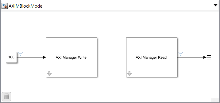
After integrating an AXI manager IP into your FPGA design, load the design on the FPGA. Then, create a Simulink model that includes source, sink, AXI Manager Write, and AXI Manager Read blocks, as in this figure.

Configure the AXI Manager Write block. Set the write Address and Burst type parameters. On the Interface tab, select the type of interface used for communication with the FPGA board by using the Type parameter. Then, click Configure global parameters to configure the global interface parameters for that AXI manager interface.
Next, configure the AXI Manager Read block. Set the read Address, Burst type, Output data type, and Output vector size parameters. On the Interface tab, select the type of interface used for communication with the FPGA board by using the Type parameter.
Run the simulation. For each Simulink step, the write block writes to the FPGA, and the read block reads from the FPGA. View the results by using the Logic Analyzer app, or directing the data to a file.
This figure shows the input and output data displayed in the Logic
Analyzer app. In this example, the AXI Manager Write block
writes 100 to address 0, and the AXI
Manager Read block reads from the same address.

See Also
AXI Manager Read | AXI Manager Write