Downlink Control Channel
Control signaling is required to support the transmission of the downlink and uplink transport channels (DL-SCH and UL-SCH). Control information for one or multiple UEs is contained in a Downlink scheduling Control Information (DCI) message and is transmitted through the Physical Downlink Control Channel (PDCCH). DCI messages contain the following information.
DL-SCH resource allocation (the set of resource blocks containing the DL-SCH) and modulation and coding scheme, which allows the UE to decode the DL-SCH.
Transmit Power Control (TPC) commands for the Physical Uplink Control Channel (PUCCH) and UL-SCH, which adapt the transmit power of the UE to save power.
Hybrid-Automatic Repeat Request (HARQ) information including the process number and redundancy version for error correction.
Multiple-input multiple-output (MIMO) precoding information.
DCI Message Formats
Depending on the purpose of the DCI message, different DCI formats are defined. The DCI formats are given in the following list.
Format 0 — for transmission of uplink shared channel (UL-SCH) allocation
Format 1 — for transmission of DL-SCH allocation for Single Input Multiple Output (SIMO) operation
Format 1A — for compact transmission of DL-SCH allocation for SIMO operation or allocating a dedicated preamble signature to a UE for random access
Format 1B — for transmission control information of MIMO rank-1 based compact resource assignment
Format 1C — for very compact transmission of PDSCH assignment
Format 1D — same as Format 1B, but with additional information of power offset
Format 2 and Format 2A— for transmission of DL-SCH allocation for closed and open loop MIMO operation, respectively
Format 2B — for the scheduling of dual layer transmission (antenna ports 7 and 8)
Format 2C — for the scheduling of up to 8 layer transmission (antenna ports 7 to 14) using TM9
Format 2D — for the scheduling of up to 8 layer transmission (antenna ports 7 to 14) using TM10
Format 3 and Format 3A — for transmission of TPC command for an uplink channel
Format 4 — for the scheduling of PUSCH with multi-antenna port transmission mode
In one subframe, multiple UEs can be scheduled. Therefore, multiple DCI messages can be sent using multiple PDCCHs.
PDCCH Restructuring
A PDCCH is transmitted on one consecutive control channel element (CCE) or an aggregation of several CCEs. A CCE is a group of nine consecutive resource-element groups (REGs). The number of CCEs used to carry a PDCCH is controlled by the PDCCH format. A PDCCH format of 0, 1, 2, or 3 respectively corresponds to 1, 2, 4, or 8 consecutive CCEs being allocated to one PDCCH.
DCI Message Generation
The base station creates a DCI message based on a DCI format given in TS 36.212 [1], Section 5.3.3.1. Each field in a DCI message is mapped in order. Zeros may be appended to a DCI message to avoid ambiguous message lengths.
DCI Coding
To form the PDCCH payload, the DCI undergoes coding as shown in the following figure.
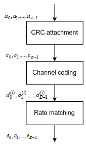
CRC Attachment
A cyclic redundancy check (CRC) is used to detect errors in DCI messages. The entire PDCCH payload is used to calculate a set of CRC parity bits. The PDCCH payload is divided by a cyclic generator polynomial to generate 16 parity bits. These parity bits are then appended to the end of the PDCCH payload.
As multiple PDCCHs relevant to different UEs can be present in one subframe, the CRC is also used to specify to which UE a PDCCH is relevant. This is done by scrambling the CRC parity bits with the corresponding Radio Network Temporary Identifier (RNTI) of the UE. The scrambled CRC is obtained by performing a bit-wise XOR operation between the 16-bit calculated PDCCH CRC and the 16-bit RNTI.
Different RNTI can be used to scramble the CRC. The following RNTI are some examples.
A UE unique identifier; for example, a Cell-RNTI
A paging indication identifier, or Paging-RNTI, if the PDCCH contains paging information
A system information identifier, or system information-RNTI, if the PDCCH contains system information
When encoding a format 0 DCI message, which contains the UE UL-SCH resource allocation, if the UE transmit antenna selection is configured and applicable, the RNTI scrambled CRC undergoes a bit-wise XOR operation with an antenna selection mask. This mask tells the UE transmit antenna which port to transmit on. The antenna selection masks are given in the following table.
| UE transmit antenna selection | Antenna selection mask, <x0AS, …, x15AS> |
|---|---|
| UE Port 0 | <0,0,0,0,0,0,0,0,0,0,0,0,0,0,0> |
| UE Port 1 | <0,0,0,0,0,0,0,0,0,0,0,0,0,0,1> |
Channel Coding — Tail-Biting Convolutional Coding
The DCI message with the CRC attachment undergoes tail-biting convolutional coding as described in TS 36.212 [1], Section 5.1.3.1. Convolutional coding is a form of forward error correction that improves the channel capacity by adding carefully selected redundant information.
LTE uses a rate-1/3 tail-biting encoder with a constraint length, k, of 7. This means that one in three bits of the output contain useful information while the other two are redundant. The structure of the convolutional encoder is shown in this figure.
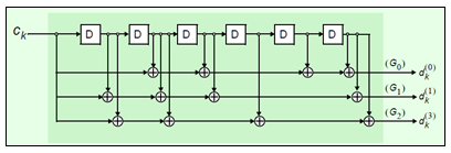
Each output stream of the coder is obtained by convolving the input with the impulse response of the encoder, as shown in this equation.
The impulse responses are called the generator sequences of the coder. LTE has these three generator sequences.
G0=133 (octal)
G1=171 (octal)
G2=165 (octal)
A standard convolutional encoder initializes its internal shift register to the all zeros state, and also ensures that the coder finishes in the all zeros state by padding the input sequence with k zeros at the end. Knowing the start and end states, which are all zeros, simplifies the design of the decoder, which is typically an implementation of the Viterbi algorithm.
A tail-biting convolutional coder initializes its internal shift register to the last k bits of the current input block, rather than to the all zeros state. Thus, the start and end states are the same without the need to zero-pad the input block. Since the step of terminating the coder has been eliminated, the output block contains fewer bits than a standard convolutional coder. The drawback is that the decoder becomes more complicated because the initial state is unknown; however, the decoder does know the start and end states are the same.
Rate Matching
The rate matching block creates an output bitstream with a desired code rate. Because the number of bits available for transmission depends on the available resources, the rate matching algorithm is capable of producing an arbitrary rate. The rate matching block interleaves the three bitstreams from the tail-biting convolutional encoder, then collects their bits to create a circular buffer. The block selects and prunes bits from the buffer to create an output bitstream with the desired code rate. The process is shown in this figure.
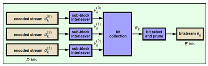
Sub-block Interleaver. The three sub-block interleavers used in the rate matching block are identical. Interleaving is a technique to reduce the impact of burst errors on a signal. It works by changing the order of bits, which prevents burst errors from corrupting consecutive bits.
The sub-block interleaver reshapes the encode bit sequence, row-by-row, to
form a matrix with columns and rows. The variable is determined by finding the minimum integer such that the
number of encoded input bits is . If , ND
<NULL>s are appended to the front of the encoded
sequence. In this case, .
The interleaver performs inter-column permutation on the matrix to reorder the columns, as shown in this pattern.
| 1, 17, 9, 25, 5, 21, 13, 29, 3, 19, 11, 27, 7, 23, 15, 31, 0, 16, 8, 24, 4, 20, 12, 28, 2, 18, 10, 26, 6, 22, 14, 30 |
The output of the block interleaver is the bit sequence read out column-by-column from the inter-column permutated matrix to create a bitstream of length .
Bit Collection, Selection, and Transmission. The bit collection stage creates a virtual circular buffer by combining the three interleaved encoded bit streams, as shown in this figure.
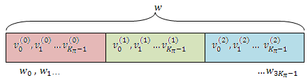
The rate matching block then selects and prunes bits from the circular buffer
to create an output sequence length which meets the desired code rate. This is
achieved by sequentially outputting the bits in the circular buffer from
w0 (looping back to
w0 after
w3Kπ–1),
discarding <NULL> bits, until the length of the output
is x times the length of the input, creating a coding rate of
1/x.
PDCCH Processing
The coded DCI messages for each control channel are multiplexed, scrambled, and undergo QPSK modulation, layer mapping, and precoding, as shown in this figure.
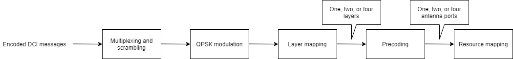
Multiplexing
The blocks of coded bits for each control channel are multiplexed in order to create a block of data, as shown in this figure.
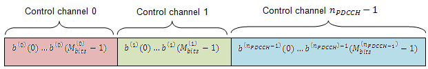
The variable is the number of bits in the ith control channel and is the number of control channels.
Matching PDCCHs to CCE Positions
If necessary, <NULL> elements are inserted in the block of bits
before scrambling to ensure PDCCHs start at particular CCE positions and the length
of the block of bits matches the amount of REGs not assigned to PCFICH or
PHICH.
The PDCCH region consists of CCEs which could be allocated to a PDCCH. The configuration of how PDCCHs are mapped to CCEs is flexible.
Common and UE-specific PDCCHs are mapped to CCEs differently: each type has a specific set of search spaces associated with it. Each search space consists of a group of consecutive CCEs which could be allocated to a PDCCH, called a PDCCH candidate. The CCE aggregation level is given by the PDCCH format and determines the number of PDCCH candidates in a search space. The number of candidates and size of the search space for each aggregation level is given in the following table.
| Search space, Sk(L) | Number of PDCCH candidates, M(L) | ||
|---|---|---|---|
| Type | Aggregation level, L | Size, in CCEs | |
| UE-specific | 1 | 6 | 6 |
| 2 | 12 | 6 | |
| 4 | 8 | 2 | |
| 8 | 16 | 2 | |
| Common | 4 | 16 | 4 |
| 8 | 16 | 2 | |
If the bandwidth is limited, not all candidates may be available because the PDCCH region is truncated.
A PDCCH can be mapped to any candidate within its suitable search space, as long as the allocated CCEs within the candidate do not overlap with a PDCCH already allocated. A simple example that shows the PDCCH candidates of two aggregation levels within a PDCCH region is shown in this figure.
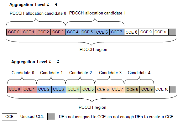
In this example, only 11 CCEs are available due to bandwidth constraints. The CCEs used to construct each PDCCH candidate are defined by this equation.
The variables are defined as follows.
— number of CCEs in a subframe, k
m — number of PDCCH candidates in a given space,
L — aggregation level
i — an integer between 0 and L–1,
When a common search space is used, is 0. When a UE-specific search space is used, is given by this equation.
In the preceding equation, A is 39,827, D is 65,537, and Y–1 is the nonzero UE radio network temporary identifier.
Scrambling
This multiplexed block of bits undergoes a bit-wise exclusive-or (XOR) operation with a cell-specific scrambling sequence.
The scrambling sequence is pseudorandom, created using a length-31 Gold sequence generator and initialized using the slot number within the radio frame, , and the cell ID, , at the start of each subframe, as shown in the following equation.
Scrambling serves the purpose of intercell interference rejection. When a UE descrambles a received bitstream with a known cell specific scrambling sequence, interference from other cells will be descrambled incorrectly, therefore only appearing as uncorrelated noise.
Modulation
The scrambled bits then undergo QPSK modulation to create a block of complex-valued modulation symbols.
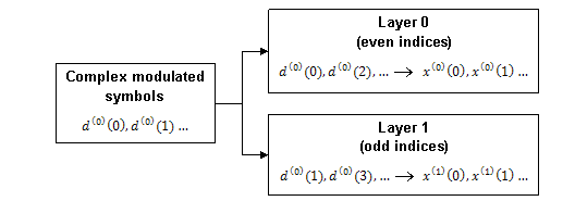
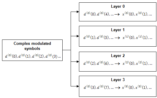
Layer Mapping
The complex symbols are mapped to one, two, or four layers depending on the number of transmit antennas used. The complex modulated input symbols, , are mapped onto v layers, .
If a single antenna port is used, only one layer is used. Therefore, .
If transmitter diversity is used, the input symbols are mapped to layers based on the number of layers.
Two Layers — Even symbols are mapped to layer 0 and odd symbols are mapped to layer 1, as shown in this figure.
Four Layers — The input symbols are mapped to layers sequentially, as shown in the following figure.
Precoding
The precoder takes a block from the layer mapper, , and generates a sequence for each antenna port, . The variable p is the transmit antenna port number, and can assume values of {0}, {0,1}, or {0,1,2,3}.
For transmission over a single antenna port, no processing is carried out, as shown in this equation.
Precoding for transmit diversity is available on two or four antenna ports.
Two Antenna Port Precoding. An Alamouti scheme is used for precoding, which defines the relationship between input and output as shown in the following equation.
In the Alamouti scheme, two consecutive symbols, and , are transmitted in parallel using two antennas with the following mapping, where the asterisk symbol (*) denotes the complex conjugate operation.
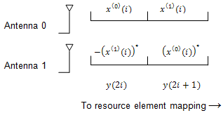
Since any two columns in the precoding matrix are orthogonal, the two symbols, and , can be separated at the UE.
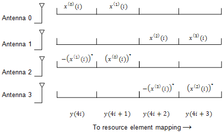
Four Antenna Port Precoding. Precoding for the four antenna port case defines the relationship between the input and output as shown in the following equation.
In this scheme, two consecutive symbols are transmitted in parallel in two symbol periods using four antennas with this mapping, where the asterisk symbol (*) denotes the complex conjugate operation.
Mapping to Resource Elements
The complex-valued symbols for each antenna are divided into quadruplets for mapping to resource elements. The sets of quadruplets then undergo permutation (interleaving) and cyclic shifting before being mapped to REs within resource element groups (REGs).
Permutation. The blocks of quadruplets are interleaved as discussed in Sub-block Interleaver. However, instead of bits being interleaved, blocks of quadruplets are interleaved by substituting the term bit sequence with the term symbol-quadruplet sequence.
<NULL> symbols from the output of the
interleaver are removed to form a sequence of interleaved quadruplets
at each antenna, .
Cyclic Shifting. The interleaved sequence of quadruplets at each antenna is cyclically shifted, according to the following equation.
In the preceding equation, the variable is the number of quadruplets, such that , and is the cell ID.
Mapping. The cyclic-shifted symbol quadruplets are mapped to REGs that are not assigned to PCFICH or PHICH.
Each symbol quadruplet is mapped to an unallocated REG in order, starting with the REG . Symbol quadruplet maps to the REG . Then, the REG symbol index, , is incremented until all the REGs at subcarrier index have been allocated. Next, the REG subcarrier index, , is incremented, and the process repeats. This mapping continues until all symbol quadruplets have been allocated REGs.
The mapping for an example resource grid is shown in the following figure.
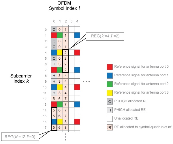
Four transmit antenna ports and a control region size of three OFDM symbols are used to create the grid. In this example, the REG is allocated to PCFICH, so no symbol quadruplets are allocated to it. The symbol quadruplets are first mapped to REG , followed by . Since there are no further REGs with , the next REG allocated is REG because this REG has the lowest value of not already allocated. This process repeats to allocate all the symbol quadruplets to REGs.
References
[1] 3GPP TS 36.212. “Evolved Universal Terrestrial Radio Access (E-UTRA); Multiplexing and channel coding.” 3rd Generation Partnership Project; Technical Specification Group Radio Access Network. URL: https://www.3gpp.org.
See Also
lteDCI | lteDCIEncode | ltePDCCH | ltePDCCHIndices | ltePDCCHSpace | ltePDCCHInfo | ltePDCCHPRBS | ltePDCCHInterleave | ltePDCCHDeinterleave | ltePDCCHDecode | lteLayerMap | lteLayerDemap | lteDLPrecode | lteDLDeprecode | lteCRCEncode | lteCRCDecode | lteConvolutionalEncode | lteConvolutionalDecode | lteRateMatchConvolutional | lteRateRecoverConvolutional | lteSymbolModulate | lteSymbolDemodulate