Post-Layout Analysis of DDRx Interface with CPU and DIMMs
This example show how to use the Parallel Link Designer app to set up a post-layout analysis of a DDRx interface on a Main Board, which has a CPU connected to two DIMM slots, to verify that waveform quality and timing margins are met by the PCB database. Most of the steps illustrated in this example are also applicable to Serial Link Designer for post-layout analysis of SerDes links.
Note: Post-layout extraction and analysis requires RF PCB Toolbox™ in addition to Signal Integrity Toolbox™. The focus of this example is to illustrate how to setup a post-layout project in Parallel Link Designer or Serial Link Designer.
Note: While there are DDR5 IBIS models in the DDRx_CPU_Dimm_Postlayout project used in this example, the circuit topologies do not represent a real-world DDR5 system and are meant only to represent an abstract DDRx interface. If your focus is specifically DDR5, see the DDR5 specific examples.
Overview
This tutorial shows how Signal Integrity Toolbox can be used to analyze a DDRx memory interface in post-layout using a Parallel Link Designer implementation kit as the starting point. This example assumes you are beginning with the implementation kit DDRx_CPU_Dimm_Postlayout by using the openSignalIntegrityKit function. This kit has Parts pre-configured for ICs such as a CPU and SDRAM. It also has pre-layout schematic sheets matching the configuration of the interface to be analyzed on the PCB database. This will allow you to begin Signal Integrity analysis immediately since all models and schematic sheets are part of the kit. If an implementation kit were not available for this interface, you would need to build the simulation environment (Parts, IBIS Models, and pre-layout transfer nets) from a new project. An implementation kit is simply a way to reuse a project once all of the above tasks have been done. For example, a copy of your post-layout kit may be used for another hardware design if it uses the same CPU, DIMM and ASIC components.
Post-Layout Verification
Post-layout verification is used to verify that the voltage and timing margins are met on the routed board. In this section you will import and set up the post-layout system, simulate and analyze the nets. Example board databases for a Main Board (file "mb.zip") and DIMM (file "dimm.zip") are provided as attachments to this example in Signal Integrity Toolbox "Neutral" format. You can acquire these by clicking the button to download the attachments and place into a folder called "boards." You can also follow the steps in this example as a guide to create a post-layout project with your own PCB databases. The following are the key points to create and configure a post-layout project.
Import and Setup Boards
Import Main Board and DIMM
Configure PCB stackup
Set voltages for IO and any active-termination nets
Configure or create Parts (which contain IBIS and IBIS-AMI models)
Create and Connect Instances
Create Instances of the Main Board and two DIMMs
Configure connectivity between Instances of the Main Board and DIMMs
Setup connector models
Setup and Run Assignment
Select CAD nets to include/exclude for Assignment to Transfer Nets
Run Assignment
Configure any Model Overrides for padstacks (vias) or Traces in project database
View Transfer Nets of interest in the boards with Signal Integrity Viewer
Configure Transfer Net Properties
Configure source-destination bus transactions in Transfers dialog
Set IBIS models for IO drive strength (ODS) and on-die termination (ODT)
Run Post-Layout Simulation
Configure PostLayout SI/Timing Simulation dialog
Run project simulation
Open DDRx CPU DIMM Post-Layout Kit
Open the kit "DDRx_CPU_Dimm_Postlayout" in the Parallel Link Designer app using the openSignalIntegrityKit function:
openSignalIntegrityKit("DDRx_CPU_Dimm_Postlayout");
Set up Post-Layout Verification
Post-Layout Verification is set up and performed from the Post-Layout Verification tab:

PCB databases will first be imported into Parallel Link Designer, then you will configure the PCB stackup information, voltage nets and models to be used. The boards are then placed into a board library which can be used across multiple interfaces. Boards from the library are instantiated and connected to enable Signal Integrity analysis of a complete end-to-end system. For this tutorial there is a Main Board and a DIMM. You will import and set up these two PCB databases, then create Instances for use in simulation analysis, and connect them together by using the Add Connections dialog.
Import and Setup Boards
Import Main Board
PCB databases are imported from the Setup & Assignment dialog. Click the Setup & Assignment button to launch the dialog.

To import a board click the Import & Setup Board button on the Setup & Assignment dialog.

This will launch the Import & Setup Board dialog with the Import Board tab active. You can select from a number of different formats of PCB database from the PCB Database Type dropdown menu. The PCB databases of the Main Board and DIMM attached to this example are in Signal Integrity Toolbox "Neutral" format, so select this option from the list.

Attached to this example are two PCB databases, which are provided in Signal Integrity Toolbox "Neutral" format as archives "mb.zip" for the Main Board PCB and "dimm.zip" for the DRAM memory DIMM. You should download and extract these .zip files into a folder called "boards" for organization purposes.
Click the Browse button, navigate to the folder where you downloaded the PCB databases, select the boards\mb\neutral directory, then select the neutral_pins.csv file and click the Open button to select the set of mb neutral database files.


Before clicking the Next button to import the board, you may want to select the "Advanced" option. This displays options for:
Creating a new Instance Name
Copying the original PCB Database to the Project folder
Set PCB fabrication options for Etch Removal Threshold
Declare Padstack Hole Size in PCB database as Drilled or Finished
Set the Padstack Plating Thickness
Determine connectivity by using CAD Rat Lines if traces are not yet laid out
Click the Next button at the bottom of the Import & Setup dialog to read in the PCB database and advance to the Stackup tab.
When the PCB database has completed importing, the Stackup tab will appear. This shows the PCB stackup information that Parallel Link Designer read from the PCB database.
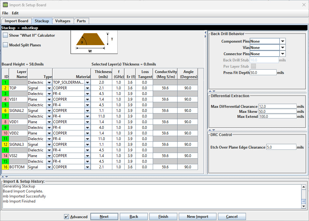
You may need to add a layer to the top and/or bottom of the stackup that represents dielectric or solder mask. Typically its depth ranges between 0.5 to 2.0 mils. You also may need to make corrections to the Dielectric Constant (Er) or Loss Tangent (or Dissipation Factor, tan δ) for layers not configured by CAD in the original PCB database.
In this case, no changes to the PCB stackup are needed, so click the Next button at the bottom of the Import & Setup Board dialog to continue. The Voltage Nets tab will appear next.
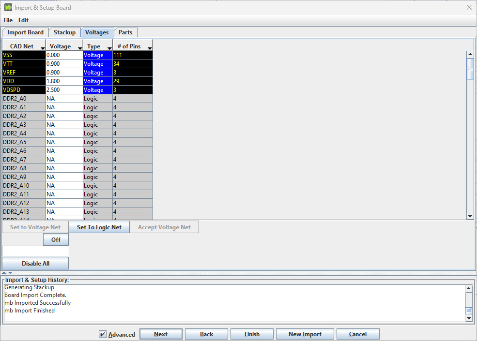
Signal Integrity Toolbox has read the voltage properties and attempts to automatically parse the voltage net names to set their values. It is important to verify the values of your specific database are correct. For DDRx analysis, correct values for VDD, VSS, and VTT are often required for correct results to be achieved. Also, if there are active terminations in the circuits to be analyzed such as a system clock or various logic families, then the voltages must be correct in order for SPICE simulations to provide valid transient waveform data. Review this list for accuracy and verify that all voltage nets have been defined as Type Voltage, and that their voltage value is correct.
All voltages on this PCB have been imported correctly. Click the Next button at the bottom of the Import & Setup Board dialog to continue.
The Parts tab will appear. A part must exist on each board or each end of an Extended Net for setup and assignment to complete successfully.
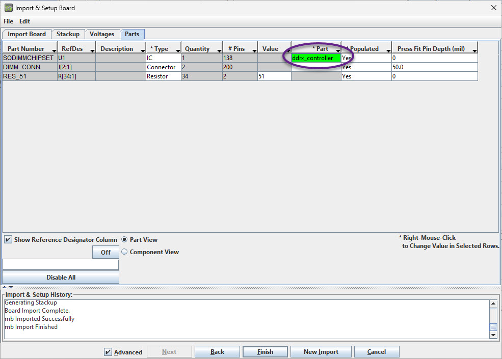
The example Main Board has devices with different part numbers on it: the memory controller, resistors and the two DIMM connectors. The Part, or library element, is filled in for the controller. Parallel Link Designer can automatically match the controller library element to the device through the part number. If you do not see the controller "ddrx_controller" listed, you can right-click and browse to it in the parts list of the project. If starting from scratch or with your own project, you may need to create a new Part in the project.
Note: You can search for parts by using a Wildcard string and toggling the button On or Off.
The Main Board is now imported and set up. Click the Finish button on the bottom of the Import & Setup Board dialog to go back to the Setup & Assignment dialog. You will see the board "mb" in the table in the Setup & Assignment dialog.
Import DIMM
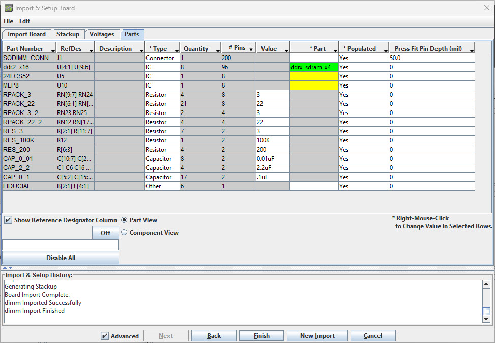
Now follow the same steps you used to import the Main board to import the DIMM board (there is a single DIMM PCB database but you will create two instances of it in the project). You may see some warnings displayed but they are beyond scope of this example and may be ignored. Be sure to verify the values on the Voltages Tab and to configure the part ddrx_sdram_x4 in the Parts Tab for the DIMM board.
You will now have two boards in the table in the Boards section of the Setup & Assignment dialog ready to create instances for connectivity.

Create and Connect Instances
Instances are instantiations of a Board used by the project to establish connectivity and setup CAD net assignment. An instance of each Board has already been created automatically when the PCB database was imported. You will need to create a second instance of the DIMM so that there are two available to connect to the Main Board. You may need to rename the two DIMM instances so that each is clearly identifiable when you setup connectivity to the Main Board instance.
Create New DIMM Instance
You need to create a second instance of the DIMM in order to connect two DIMMs to the Main Board. First highlight the existing dimm board instance in the Instances area of the Setup & Assignment dialog, then click on the Add Instance button.

Change the names of each DIMM instance to slot1_dimm and slot2_dimm (as shown in the Figure above).
Connect Instances
The DIMM instances can now be connected to the Main Board. In the Connections area of the Setup & Assignment dialog, click the Add Connection button to launch the Add Connection dialog.

To create the connection for DIMM slot1, select Instance mb in the left hand Instance list.

Note: Enable the Advanced checkbox to view additional connection options. The Probe Connectors option automatically puts a probe at the connector during simulations (when supported), while the Edit File & Subcircuit option allows you to manually enter a file name or subcircuit name when selecting a SPICE Model.
Click the Browse button to select a connector on the Instance mb. The Choose Connector dialog lets you select the connector on the Instance mb that will be connected to the DIMM. Select J1.

Click OK to close the Choose Connector dialog.
Now select the Instance and connector for the other half of the connection on the right-hand side. Select the Instance slot1_dimm and the connector J1.
The last thing to specify for the connection is the connector model. You can select an Ideal Transmission Line, Spice Model or S-Parameter file. In this example, the connector is modeled as an ideal transmission line model.

Click OK to complete the connection.
Now create a connection between the Main Board and the second DIMM:
1. Click Add Connection.
2. Select Instance mb and connector J2 on the left.
3. Select Instance slot2_dimm and connector J1 on the right.
4. Select ideal transmission line connector model.
5. Click OK to complete the second connection.
The Connections area of the Setup & Assignment dialog should now have two connections in the table, as shown in the figure below.

Setup and Run Assignment
Now that the connectivity is specified, Parallel Link Designer is ready to extract the connectivity from the multi-board system. Parallel Link Designer will match the nets extracted from the boards to the Transfer Nets already present in the Design Kit so that the Transfer Net properties can be used in simulation. This process is called Assignment. By default, all nets will be extracted from the PCB database(s), however to speed things up, you can select which nets to include in the assignment using the Assignment Setup button.

This brings up the Assignment Setup dialog:

In this dialog, you can use the filter and wildcard entries at the top of each column to find nets to include in the simulation. For example, you may want to select only DDRx-related nets for a larger PCB database if it contains thousands of CAD nets. This would reduce the database size in Parallel Link Designer and optimize other operations for speed. Since this is a small database, you can leave everything as-is and close the dialog.
To run Assignment, click the Run Assignment button on the Setup & Assignment dialog.

When the Assignment process is complete the Assignment and Validation Reports are created.

It is always a good idea to check the status after running Assignment. It can alert you to problems that may be difficult to debug without seeing the error messages. For example, if there are warnings listed they may represent unused parts. Even if you see no errors or warnings it is wise to review the reports so that you clearly understand the project status.
Note: You can use custom models (such as SPICE subcircuit or Touchstone s-parameter files) in your PCB database for traces and padstacks (vias). The button is enabled for opening the Padstack/Trace Manager after Run Assignment has completed.

This allows you to see all the Padstacks(Vias) in the design. You can right-click to open the Via Model Editor, and check the option to use set a Model Override for a padstack (via) or trace instance or by occurrence (e.g. to override all padstacks having the same library name).

Click the Ok button to close the Via Editor dialog.
Click the Close button to close the Padstack/Trace Manager dialog.
Click the Close button to close the Setup & Assignment dialog.
Complete Post-Layout Setup
After Assignment is complete, on the Post-Layout Verification tab there will be a table with all of the extracted Extended Nets listed. You can use the Viewing Filters to Vectorize nets or to Hide nets where Simulate = N/A. For example, when nets are Vectorized, all of the dq nets are in one row, and all of the dqs nets are in another row. The option for Hide if Simulate = N/A suppresses any transfer nets that are not valid or otherwise unsimulatable in the current set of assigned nets.

To view any set of nets on the board, highlight the rows you want to see and select Show on Board from the right-click menu.

This will launch the Signal Integrity Viewer with all the selected Extended Nets highlighted.

Configure Transfer Net Properties
In this project, the nets from the boards have been automatically matched with the Transfer Nets that have already been set up in pre-layout. This allows the post-layout simulations to make use of the bit time, bus transaction definition and model overrides (for on-die termination) that were part of the Transfer Nets in the original project. You can configure the Transfer Net Properties to define Transfers between a DDRx controller and DIMM or DRAM. You can also set clock or symbol UI, drive strength (ODS) and on-die termination (ODT). Click the TNet Properties button to bring up the Transfer Net Properties dialog.

The nets are now ready to simulate. By matching the nets on the board with the existing Transfer Nets, Parallel Link Designer has reduced the post-layout task to importing and setting up the boards in the system. Parallel Link Designer will automatically extract the actual routed topologies, simulate and analyze each net according to its respective Transfer Net properties, normalize and measure interconnect flight times and compute timing margins for the appropriate transactions.
Run Post-Layout Simulations
By default all nets are excluded from simulation in post-layout. To select all of the nets and include them for simulation select all of the table rows and click the Include button in the Extended Net Simulation area.
The Base Spice Simulation Count field in the lower right shows the number of simulations. This will change depending on the number of Transfer Nets, Model Sweeps, and Corner Conditions selected for your simulation.
Click the Simulate toolbar button: or select Run | Simulate from the menus to launch the Post-Layout SI/Timing Simulation dialog. If you are asked to save changes, click Yes. Select all check-boxes applicable to the type of DDR in your design (e.g. Analyze Timing does not apply to DDR5 but does apply to earlier versions such as DDR3).

Click the Run button to start the simulations.
Note: The simulations may take several hours to finish. To speed up simulation time, you can use Parallel Computing Toolbox to run simulations in parallel. For more information on setting up Parallel simulations, see Run Parallel Simulations in Signal Integrity Toolbox.
When the simulations have completed, Signal Integrity Viewer and the spreadsheet report will launch. As in pre-layout there are waveform tabs and timing tabs. To interpret the results, see Results of Pre-Layout Analysis in Parallel Link. Note that since the Main Board does not represent a real-world DDRx interface implementation, there may be many waveform violations.