Optimize FPGA and ASIC Speed and Area Using HDL Coder - MATLAB & Simulink
Video Player is loading.
Current Time 0:00
Duration 41:21
Loaded: 0.40%
Stream Type LIVE
Remaining Time 41:21
 
1x
  • descriptions off, selected
  • en (Main), selected
    Video length is 41:21

    Optimize FPGA and ASIC Speed and Area Using HDL Coder

    Overview

    Learn how to use HDL Coder optimization and design techniques to meet your target-specific speed and area goals. HDL Coder offers techniques that span from automatic to fully-controlled, and all of them allow for rapid exploration of implementation options. This webinar will explain these options and their associated benefits and tradeoffs, including verification considerations, and will discuss techniques specific to FPGA and ASIC designs. All of these techniques will be demonstrated using the pulse detection design from the HDL Self-Guided Tutorial.

    Highlights

    • Workflow options from rapid estimation to running full synthesis and implementation
    • Optimizing for speed
    • Latency vs throughput vs clock frequency
    • Pipelining techniques
    • Vector processing
    • Multiplier mapping
    • Optimizing for area
    • Resource sharing
    • RAM mapping
    • Loop streaming of vector operations

    About the Presenter

    Eric Cigan is a principal product marketing manager at MathWorks for ASIC and FPGA verification. Prior to joining MathWorks, he held technical marketing roles at Mentor Graphics, MathStar, and AccelChip. Eric earned BS and MS degrees in mechanical engineering from the Massachusetts Institute of Technology. In his spare time, Eric curates a wide-ranging, ever-growing collection of FPGA development boards from manufacturers around the world.

    Recorded: 28 Jul 2022

    Hi, and welcome to this session on Optimizing FPGA and ASIC Speed and Area using HDL Coder. I'm Eric Cigan, and I'm responsible for technical and product marketing for our FPGA and ASIC products here at MathWorks including HDL Coder, and I've been at MathWorks for 15 years working in the area of FPGA and ASIC design and verification. Before that, I worked at Mentor Graphics and a few EDA and FPGA startups in product marketing, technical marketing, and application engineering roles.

    My degrees are in mechanical engineering with a focus on control system design, but the focus for today's session isn't on that nor is it actually on learning HDL Coder. The basics of HDL Coder are covered really well in a tutorial that I'll point to a little bit later on. But the focus here is to really help you try to understand the options you have for optimizing your results and it's really going to be dependent on your particular applications needs and your methodology.

    It helps to start out with just understanding what your application's goals are. One of the terms we'll use here is latency, which is the lapse of time or clock cycles between when inputs come into your design and when they're processed and coming out the output. So if you think about an application like a control algorithm for a high-speed electric motor or an antilock break sensor, those cases, you really want to minimize the processing time. In other words, you want low latency.

    On the other hand, for some of the more modern automated driving applications, for instance, that require really high throughput, and that's just the sheer amount of data that you can process. So if you consider like a camera input, or a lidar, or even radar, where you've got large frames of images with varying levels of intensity or color, well, in those cases, you need to process a lot of data. And on top of that, with a lot of applications, you'll have requirements for small form factors whether you're trying to fit into something like a CubeSat satellite or just a handheld device.

    And for high-volume applications, you'll want to use the smallest device possible simply for cost reduction. Then, of course, power is always a consideration these days, whether it's just for portable products running off of batteries or for heat removal. Ultimately, power is a product of how many resources you have on your device and how often those are used, so higher switching speeds will tend to consume more power.

    OK, and then just a brief introduction of HDL Coder. HDL Coder works within MATLAB and Simulink. Typically, our customers use Simulink for hardware design because it has a native built-in sense of time and parallelism, and it's a nice visual application where you can visualize your hardware architecture. We can also take in Stateflow charts or like finite state machines, as well as reused Verilog and VHDL IP and implement that as part of your design.

    Because of its high-level visual nature, Simulink makes a good collaboration environment between algorithm developers and hardware architects so they can work together to refine the design toward hardware. And then you can automatically or manually convert to fixed-point or you can stay in floating point to generate your hardware either way. So we're going to focus a lot today on customizing these optimizations that are available to you in HDL Coder and then show how it generates readable synthesizable HDL.

    And you can also if you've got functional safety requirements, trace it back to your requirements. And because Simulink is this high-level design environment, it makes it really easy just to regenerate your code depending on your different requirements, and that's one of the factors we'll look at today in terms of choosing your optimizations.

    But first, just some concepts of terminology that we'll use today. We'll illustrate initially with this very simple 4-tap FIR filter. Of course, you can see the math box here, the adders, and multipliers, but you also see these delays here. Now, the delays in this particular design, we would call these design delays because these are really necessary for the design to operate properly. That's because in hardware, in the real world, you can't just perform math on an entire signal or entire matrix at a time.

    Hardware streams in sample by sample by sample over time, and as these sample stream in, well, if we didn't have these delays the data would just cascade through the logic in an unpredictable way and we wouldn't be able to control what's being added to what or what's multiplied with what. So if we use these design delays, we can manage that data flow allowing them to stream in one sample at a time.

    Now, If you're familiar with Simulink and its sample times, you'll note what's actually set in the sampling time is in terms of time units. Here though, we're really just relating them to clock cycles in hardware. And these design delays will ultimately map to registers in hardware. You'll see us use terms interchangeably-- delay and register-- but when you think about it, either way, they just signify one clock cycle.

    You'll notice now that we've clocked in two samples and we actually get a result on that output. So that's what's actually going to be a term that we use here as well. We'll call that latency. So that's a latency of one clock cycle. And then another pair of terms that we'll use here are input pipeline and output pipeline. And the reason we use these is it's just a good design practice because this logic takes some time for signals to propagate through.

    And we don't know the signals coming in. We don't know where they've been. We don't know exactly where they're going to arrive. So it helps to be able to synchronize those with these input registers. And similarly, on the outputs, this logic is going to go somewhere else and merge in with some other logic. So if we synchronize the outputs, then we know that they're all going to arrive at the next operations at the same time. But now because we've added this additional register on the output, we've added an additional cycle of latency. So now, our latency, as you can see here, is two clock cycles.

    The other important piece of information to understand is critical path timing. I mentioned that this logic takes time for signals to propagate through. You can see an estimate of the critical path that the HDL Coder gave us and how the multiply is actually a larger consumer of time on this. But our critical path is the longest path through the design, and this becomes a gating factor for how fast we could actually run our clock.

    So this logic up here has no real logic between the registers, so it can run really fast. But as our filter grows-- I mean, you think this is only a 4-tap filter-- if it starts to grow, this critical path length is going to grow as well and it's going to become a real gating factor in how fast we can run our design. So here, we had this particular configuration. The latency in terms of time is going to be two clock cycles, just over five nanoseconds, so it's going to be just over 10 nanoseconds overall.

    But we have this problem where the critical path is going to grow as we grow our filter. So we can break that up by just putting these pipeline registers after each of the adders, and now, that basically fixes our critical path timing. So no matter how large this filter grows to, we'll always be able to run it at the same speed. And here, our critical path is through a multiply and one adder, so we end up with this propagation delay of 3.83.

    But we did also add extra cycles of latency. So now however long this filter ends up being, we're adding in cycles of latency. But at least, we always know that we can run this at a given clock speed, which is often important for keeping up with being able to process inputs coming in like data coming in off of an A to D converter. So here, our latency is four times 3.83, so it's about 15 nanoseconds in time units. But as I mentioned, we can run a clock a lot faster to keep up with incoming data rates.

    OK, and then throughput, I referred to that earlier as well. It's really just how much you can process in a given amount of time. The nice part about hardware is you can process data in parallel. The price you pay is that more parallelism means consuming more hardware resources, so the amount of resources you use will grow, but you do have the advantage of being able to process a lot of video data or radar data coming in at a given time without having to drop data just to keep up.

    That means you can process more data with a given clock frequency or you can even reduce your clock frequency a bit. And the reason you might want to do that is to reduce power consumption. So if you only need to process four sets of data in parallel, if you increase your parallelism to eight and then the clock speed half as fast, you're actually trading off the power that gets increased by the increased amount of logic.

    These are the sort of design decisions that you can explore in an environment like Simulink. It's a lot harder to do when you're hand coding RTL, but it's pretty easily done in this high-level environment. And then it also helps to understand your target hardware in terms of the resources they had available. Any particular FPGA has a fixed amount of resources. You can see some examples here. One key bit of resource are these IP blocks which we'll cover in more detail in a moment.

    With ASICs on the other hand, you'll have a lot of reused IP in macros like RAMs and processors, but where you're developing your new algorithm is really up to the designer. You'll have some options in terms of the cells you map to, but when you're designing an ASIC, you have more freedom than when you're using an FPGA. But with that freedom, you're taking on a much harder and more expensive implementation methodology.

    The hard IPs and FPGAs that I spoke about on the last slide, they can go by different names, but with each of the FPGA vendors, they use slightly different terminology. So for instance, AMD/Xilinx refers to DSP slices. Intel will call them DSP blocks. And Microchip call them math blocks. And I'll probably use them interchangeably here, so apologies to those three very good companies.

    But it's really important to understand these capabilities because in algorithm design, multiplication is heavily used, and that can be very expensive to implement in hardware. But these hard IP blocks implement it very efficiently. So this composite image I use here shows what's pretty typical. At the center is a multiplier. Quite often there's a multiply-accumulate capability and an optional pre-adder, as well as registers scattered throughout so you can run these at very high speeds.

    The other important consideration to look at is the word length of the input. So this is important to understand. Earlier generations of FPGA devices tended to support 18 by 18 multipliers or 18 by 18 operations, but the newer ones do support wider word lengths. So this is important to pay attention to when you're trying to map your multipliers efficiently on FPGAs because these resources are pretty precious. We look at how we manage these in this example, a design that I'll cover in a moment.

    As I mentioned, with ASICs, when you're mapping to multipliers, and, again, it's pretty wide open, you should try to keep it to a power of two. Equivalence checking is a consideration to keep in mind with ASIC multiplier implementation. These pipeline stages, it really helps if those are already distributed throughout the logic in your RTL before you go to synthesis. It also helps to keep your operation smaller. It's just a smaller problem for equivalence checking to chew on, and it also helps with speed because place and route tools, when they place the cells, they can spread them out more and create a self-buffering type of path.

    So for ASIC, one of the things you can have is really fine-grain control over your multiplier implementation. Here, we're showing the HDL block properties for a specific multiply, and you can use this ShiftAdd implementation, which is a smaller implementation that the place in route tools can spread out very nicely for speed.

    So I've referred a little bit to these implementation stages. HDL Coder works, again, within Simulink, and it generates Verilog or VHDL, and that goes into a synthesis tool, and the synthesis tool will take that and map it to actual cells specific to your target device. It will optimize for timing but it really only knows the timing of the cells at that point. It doesn't really know how to be placed and what the routing delays will be, so it will use some estimates for that. Then when you get to an implementation, it actually places the cells and connects them with wires, and all those wires have delays.

    So given that, implementation is really where you get the most accurate sense of what your actual timing is going to be. And you can back-annotate this timing information back into Simulink to see where your critical paths are. But synthesis's runtime, of course, is much longer than HDL code generation, and then implementation takes even more time than synthesis, so it really helps to be able to do your iterations more tightly up here within HDL coder.

    One of the things we'll look at is that on the way to generating HDL, HDL Coder will generate this generated model, which shows you how it's actually implementing its optimizations, and that can be really helpful. And when you're using automated optimizations, it helps to understand an estimate of the critical path timing. To do that, you need your cell library to have the timing characteristics for HDL Coder to work with. HDL Coder provides a lot of device timing characteristics out of the box.

    You can check the documentation to see what's supported, and it will be some defaults if you don't have the data for your device, or you can manually enter it for your given device. It uses it to show you this critical path estimate report, but it also uses it to fine-tune its optimizations as it's running. We'll take a look at that in the example design.

    We'll start off with just how to optimize for speed and show you the trade-offs between increased automation, which allows you to more easily implement your design and explore a wider variety of options more quickly, and it makes your design more portable versus manually doing it, having more control over the optimizations and being able to simulate the effects at a high level before you go and implement.

    One more note for many of you. Safety certification workflows often require the functionality be designed in, so it's traceable back to requirements, and you can simulate everything properly upfront. These are the types of trade offs to think about as you're looking at these optimizations. As we walk through this example, we'll start with more fine-grained control.

    This example is in our tutorial, and the easiest way for you to find it is just in your search engine, type in HDL Coder tutorial, and you should find that fairly quickly. It really does a nice job of teaching you how to use HDL Coder. OK, so the design here is really just a pulse detector and they're commonly used in wireless and radar applications. So it starts off with a matched filter, which takes in a known pulse, and basically, tries to match it with an incoming stream of signals.

    So this is a FIR filter, which has been pre-implemented for us. And it's a piece of IP that ships in our DSP HDL Toolbox. And it offers a variety of implementation architecture, as you can see here. Depending on the architecture, and the number of coefficients, and so forth, it will show you what the actual latency is and it will simulate that. And the output of the filter, what it's doing is to try to find where the match is. And the reference algorithm, it's doing a max on the absolute value of this complex signal.

    You probably remember that the absolute value of a complex signal is the complex magnitude, which is the magnitude of the real and imaginary parts. So for those of you who aced Pre-Calc, you're probably saying that that's a two norm. But anyway, it's the square root of A squared plus B squared, which is all familiar to many of us. So this is where it really helps to have your hardware architect working closely with your algorithm designer because the hardware developers understand that implementing a square root in hardware is really expensive, both in terms of resource usage and timing.

    And the algorithm developer knows that we don't really care about the actual result of the square root, we only care about the relative magnitude. So it turns out we really don't need to perform the square root. We can just square the inputs and add them together and that will do. So that's what we do in this pulse detector in this block labeled Compute Power. We'll visit that quite a bit here. Also, you notice that before we get to multiplying the real and imaginary parts, in the middle of the screen, we have this convert block to reduce precision down to 18 bits for the inputs.

    So again, this is keeping in mind that since 18-bit DSP blocks are ubiquitous in FPGAs, that would make a design like this very retargetable to different FPGA families. So here, I'm actually going to target a particular DSP slice on the Xilinx UltraScale+ family. And I've had some experience working with those, so I know that for this particular configuration, I can get some pretty high speed in terms of frequency by having two delays after the multiply and one before because I'm not using a pre-add function.

    And then the local peak subsystem basically tries to have a rolling window. It looks at the last 11 samples, and finds the peak amongst those, and compares it to a given threshold. OK, so now, we move to HDL Coder, and I'll bring up this workflow advisor tool because I'm going to use this to run FPGA synthesis in the implementation with the vendor tools, from AMD/Xilinx in this case. So again, I'm not going to walk through all the steps in this workflow advisor, but I do want to show that we are targeting Zynq UltraScale+ family here.

    I've set the target frequency for 500 megahertz just to push it to see how fast we can go. And for this particular device, it's a minus two-speed rate. I've got a characterized timing database for this, so we can use that for our critical path estimation. At this point, we can just generate HDL and see what a critical path looks like. So this report shows an estimate of our critical path. As you see here, it's really just a multiplier. So we can actually highlight this in our model to see where it's coming from, and this is in our compute power subsystem that we looked at before.

    So notice the numbers here. For a 500 megahertz target, that's two nanoseconds from path timing, so we'll see how this plays out. HDL Coder is typically pretty conservative with its timing estimates, but I think as we run this through implementation and it starts mapping to those DSP slices, we can find they'll run much faster than what it's showing for these estimates. That would take about 20 minutes or so, so we can skip ahead to a completed run. And here's our results after implementation.

    So as you can see in this timing summary, we did pass timing. We actually exceeded our target FIR clock frequency reaching nearly 530 megahertz. So if we look at what the gating path is in terms of timing, it's always helpful to pull up these timing reports. OK, so if we scroll down and look here, here's our path. So it's actually in the peak detection subsystem, the subtraction operation. So we'll work with that in one of these example designs coming up.

    In the meantime, I also wanted to just go back and show why I ran all the way through implementation. If we look at just the post-synthesis results, we actually see a similar data path delay. It's saying that we have a negative slack though, and that's because synthesis builds in some amount of margin. In fact, when we look at the synthesis timing report, you'll see here that inside this filter, we have this large delay that's really just a net.

    So this is really all about this one net and it's because there's a large amount of fan-out. So remember I said that after synthesis, synthesis doesn't have any notion of what the delay is due to routing, so it makes these statistical estimates based on how much a net fans out. So it's really just an estimate here. Here, it was probably a little bit conservative because the FIR filter ended up being able to run at a very fast rate. So again, our critical path was in the subtraction operation, so we'll come back and look at that later.

    But first, let's step back and look at what HDL Coder can do at the other end of the spectrum from what we just did in terms of manually designing everything. Let's look at how it handles things with automated optimizations. So here, you'll notice in that Compute Power block that we have not designed in any of the delays. So we're going to turn on an HDL Coder optimization called adaptive pipelining, and where you would set that up is under the optimization settings, and pipelining, and we turn on adaptive pipelining here.

    Now, what this does is it uses those delay estimates, the critical path estimate, combined with the target frequency to figure out how many delays it needs to insert to optimize and to try to meet that target frequency. The other thing we're going to do is that subtraction operation on the critical path was in this MATLAB function block. So this is just MATLAB code. It's hard to see how this would work in terms of timing.

    So what we can do here is go back to the HDL block properties, and I set this architecture-- by default, this is a MATLAB function-- but I'll set it to MATLAB Datapath. Now, when we generate the design, this will actually generate a Simulink version of this, and we can take a look at the timing. So here, we're just going to generate the HDL code and see what happens in terms of the automated optimizations that HDL Coder does.

    So we have our results, and I mentioned that we turned on adaptive pipelining. Now, if we look at the report here, you can see that it inserted two pipelines at each of the multipliers, and we can see how that plays out with that generated model that I was talking about before. If we go into that compute power subsystem, you can see that it put one pipeline stage before and after the multiplier.

    Now, remember, I designed in two after the multiplier because that's what I wanted based on what I knew about the DSP architecture. So we'll revisit that in a moment. You'll notice also that it put in this delay match. So when it adds the pipeline delays here, it needs to match them on parallel paths. It does that automatically. We can take a look inside this local peak subsystem here.

    So first of all, you'll notice this is how a tapped delay gets expanded. So essentially, this is just delaying the input signal and taking each state of these and combining them into a vector to go into that MATLAB function block which is here. Here, you'll notice here's our subtraction operation that was on the critical path last time. And there are no pipeline stages. It has some logic after it, so we might be able to improve this, so we can try some things in a kind of a semi-automated state.

    But just looking at the results of this, when I run it all the way through the implementation, we actually got pretty similar clock frequency to that manual implementation. So this really shows you the two ends of the spectrum. This was much more automated, but we didn't get the exact placement of the delays where I originally intended. But we were able to get pretty similar clock frequencies. It really comes down to your methodology.

    If we look at the timing report for this critical path-- I already have it pulled up here-- again, it's in that subtraction operation. OK, so let's see if we can get some delays into that even though it's a MATLAB function block. So here, what we'll do to get delays into this part of the logic that's on a critical path is I'll bring up the HDL block properties. And again, we'll set this to MATLAB data path, so it allows it to take part in the optimizations. And we can see what those will look like in the generated model.

    I'm going to add this constraint for output pipeline, so it's going to just insert two pipelines in the output and one in the input. And I've also enabled distributed pipelining which will allow HDL Coder to move those pipelines throughout the logic and place them where needed based on the timing. One other option here, you'll see this is a constrained output pipeline. If I specify something here, that will make sure-- see, I put a one there-- that will make sure one pipeline stage stays at the output even when I'm distributing them throughout the logic.

    It will force one to stay at the output for synchronization purposes, like we were talking about earlier, with that FIR filter. I'm going to leave that there for now. So we can turn that on. I'm also, in compute power, I'm going to have it insert three on the output and distribute those. And when you're doing this sort of semi-manual approach where I'm actually specifying the number but letting HDL Coder distribute them, we're still inserting those during the HDL generation process.

    So it's a good practice to document that you're doing this. But again, this does allow for flexibility in terms of exploring a wider range of options, so we'll see how this turns out. So first, let's take a look at the generated model from HDL Coder and see what optimizations it applied. We were interested in looking at the local peak and specifically, in that MATLAB function.

    So and here now, you can see that it added the three pipeline stages and it distributed them across the entire logic here. So you'll see our subtraction operation, which was on the critical path, really is bounded by two pipeline stages. So this longer path that went through all the logic, that shouldn't be a getting factor anymore. And back in the compute power subsystem, remember, we gave it three delays and let it distribute those as it saw fit.

    So instead of putting two after the multipliers, I had done manually, it actually spread these across the adder, so we'll see how that turns out. In the interest of time, I've already gone and run the implementation, and you can see the results here. The clock frequency is still over 520 megahertz. It's not quite what we achieved with the manual implementation, and let's just see where the critical path is at this point.

    Looking at this, it's actually in the FIR filter now. We've moved it off of the subtraction operation and it's in the FIR filter, and really the reason, as we saw before, is that it has to do with that high fan-out net. In this case, we've already placed and routed it so the routing delay here is real. This is really where the bottleneck is at this point and we don't have a lot of control over that. That's one of the trade-offs with using off-the-shelf IP.

    There are some pretty optimal implementations, but if I wanted to push this further, I'd probably have to design my own FIR filter. And I'm not sure I want to be up to that task, especially from a verification point of view because now, I would need to verify it. So this is about as good as we're going to get here with this particular FPGA target. But let's take a look at ASIC implementation of this.

    So first off, running ASIC synthesis requires me to be on Linux so the graphics may look a little bit different, and also, the ASIC tools tend to be more batch-scripting based, so we ran in a scripting mode here. But that also allowed me to experiment a lot, and I arrived at some settings here for implementing on ASIC where I just let the tool insert pipeline stages. So I specified an output pipeline stage count of 12 on the compute power subsystem, and I'm going to set the multiply architectures to ShiftAdd.

    And so this is happening here where I'm searching that compute power subsystem for multiple blocks and applying those settings. This allowed me to do some exploration. I also set up an HDL Coder to just run and batch, so use this read HDL. For every file that gets emitted, it will emit this command to read HDL into the script, which I then integrate with my ASIC synthesis script where I already have a clock setting set up in my library loaded.

    So I'm targeting here at TSMC 28 nanometer standard voltage threshold library. I actually tried cranking it up to a gigahertz. So my target clock period was one nanosecond, or in this case, I'm using Cadence's Genus Synthesis. They use units of picoseconds. So you'll see we set it for 1,000 picoseconds for the clock period. And I met timing right on, so Cadence's Synthesis tools will go for timing, and when they meet timing, then they'll go and recover area.

    So you could see we're able to achieve gigahertz clock speeds with this, at least out of Synthesis. Place and route might be a different story. I'm not about to try running ASIC place and route, but you can see that there are a variety of ways to achieve your goals depending on what your methodology is and how reasonable you want your design to be. OK, next, we're going to look at a different approach and talk about throughput. To increase throughput, we've actually adapted the pulse detector design to process two samples in parallel as a vector of two, which you can see here going into the design under test.

    I'm using this buffer block to create the vector, and so now, we're able to take an existing stream and sending out two samples at a time. So this is actually a slower data rate going into the pulse detector. You can see here with the sample rates, the green one has a period of two, but, again, since the entire pulse detector shows up as green in Simulink, it's all one sample rate. When we go to synthesize and implement this, we'll run into whenever clock rate we want.

    So here, you can see this vector of two going to the FIR filter. Our DSP HDL Toolbox box support any number of vector inputs, two, four, eight. And all you need to do is just change the data coming in, and it will automatically adapt. You can see now the latency is less because it's running more in parallel, but this automatically handles it. So you can imagine how quickly you can just explore trade-offs or throughput versus resource usage.

    Then similarly here, the multiplications and additions all natively support vector processing as well. The only change I had to make to this design was the tap delay, which was creating that window of delays because I have them coming in parallel. When we create the tap delay, we just needed to interleave them, so we designed this manually. But other than that, it was pretty easy to set this up to process two streams in parallel. And I've already gone and generated the code, so we can take a look at that HDL code here.

    It's all linked, and you can see everything is vectorized. There are data inputs for real and imaginary parts. There's a vector of two here, so it's like everything is duplicated here in the RTL. I've already run this all the way through to implementation. And you can see here, this was still able to achieve a clock frequency of nearly 520 megahertz.

    But now, we're processing two samples at a time, so our input is processing not just 520 megasamples per second, it's now over one gigasample per second. And with the sorts of ADD converters that are available nowadays that can produce data streams coming in at those rates, it's really great to be able to process those on the front end at such very high sample rates. Then if you wait, you can always reduce your sample rate later.

    So now, let's focus on optimizing for area or resources if you think about it that way. So you can do this manually in your design, but we're going to show some automated techniques here, and it's really about reducing the amount of resources that are used. So going back to our FIR filter example where we had those four multipliers in parallel, what if we could share those and just use one multiplier rather than four? Well, to do that, we need to convert these parallel samples into just one stream of samples and then time multiplex this multiplier.

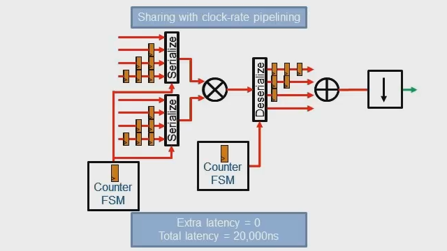
    To do that without adding a lot of cycles of latency like if we were going to share eight of them, we would end up having to increase it by a lot of cycles of latency to serialize it. Instead, what we'll do is to oversample this logic, so the serializer and deserializer logic manages that for you automatically. What we'll do is we'll run this section of logic four times faster than our base rate. So we only end up with really one extra cycle of latency on our base rate, and I'll show you what that looks like.

    And again, here's our FIR filter with our four parallel multipliers, and I'm going to specify to share all four of those. The way we do that is on the subsystem, we'll bring up the HDL block properties, and we will specify a sharing factor of four. What that does is it will identify groups of four multipliers to share as one.

    We can look at the sharing report, and we can see that our group size was four. It shared a product. So we can highlight what got grouped together and shared so we can see this here. So this is our original Simulink model. It's just highlighting the sharing groups linked to the generated code with some comments as well, and we can also look at the generated model. I'll just turn on Sample Time Colors to visualize this because this shows how it oversamples that sharing logic.

    You can see the period here, the red is four times as fast as the green, so it's oversampling by four, and you can also see this multiplier is associated with sharing group number one. An easy way to share resources for heavily vectorized operations is a technique called streaming. It requires a heavily-vectorized design, so I'm just going to use this published example to show this off.

    So this example design is pretty simple. There are only three gain blocks, but it's vector data of 24 going into each of them. So if we were going to just generate HDL code for this, we'd end up using 72 multipliers. To do this, we'll bring up the HDL block properties, and similar to the sharing factor, we'll set a streaming factor of eight, and this will create groups of eight multipliers when we generate our HDL code. We'll get that started.

    OK, and in our code generation report, similar to sharing, you can see the settings and what this created, and we can highlight that in our original design. You can see everything that it streamed here. And if we look at our generated model, similar to sharing, you can see those highlighted as well. And you'll notice the colors here. We are sharing groups of eight, so our oversampled rate is eight times faster than our base rate.

    And you can see in the model here, so we'll end up with these three multiply blocks as a result. We can see those better if we zoom in here, so here's one, two, and three. We have a vector input of three coming into these, so when we look at our final high-level resource report, we'll see nine multipliers.

    Let's cover one more optimization here that's mapping pipeline delays to RAM, and that can help a lot with resource considerations and trade-offs. In this example, you'll see some large delays like this in designs, for instance, that are keeping track of a moving average as you would do with keeping track of a threshold like in that case of the pulse detector we saw earlier. For instance, looking at the last 50 samples and keeping a moving average window, it's probably storing here, in this case, the sample that was 50 samples ago, and then subtracting that off of a rolling sum.

    A design like this would get implemented as 50 distinct registers, and these samples will clock through the registers as it goes. In your design, if you want to conserve registers, for instance, if you're on an FPGA and have plenty of RAM available but not enough registers, well, then you can map these pipeline delays to RAM, and it will end up looking something like this. If you're designing for an ASIC, this can also help because in ASICs, your RAM is going to be more tightly packed, and you can generate whatever sized RAMs you want.

    OK, so let's take a look at some of our customers' experiences with our optimizations. Here, we've got a variety of customers and the types of approaches they use. For this first customer, comparing in gray their manual hand-coding approach and all the times and metrics are indexed to one for the results for hand coding. So their die area, in this case, they spent a lot of time manually writing optimized RTL. This was an ASIC customer, wireless, and very high-volume application. So with HDL Coder, they were able to achieve the same die area but in less than half the time because of their ability to just explore architectures at a high level and then implement those.

    Here's another ASIC customer that was developing an automotive application. And as you can see here, by using HDL Coder's optimizations and being able to explore their architectures at a high level, they were able to reduce area and power usage by quite a bit. This third customer was developing a vision application for an FPGA, and you can tell that they probably did a lot of their architecture exploration because, in a fairly short amount of time, they were able to save a lot of resources on their FPGA, and that was pretty important to them.

    And finally, this fourth customer was comparing use of HDL Coder versus their manual hand-coding approach. They were developing an FPGA prototype for an ASIC application, and because they were able to optimize their pipeline insertions, they were able to run their clock a period much, much faster. In terms of area, they also improved by 40% because of all this exploration.

    So that's really the power of HDL Coder. It gives you the ability to explore, measure at a high level, have these tight iterations within this high-level environment no matter what your goals are, and then just generate and regenerate code as needed for whatever your particular project or target needs are. OK, so thanks a bunch for your time today. I hope this was helpful in helping you understand what techniques might suit best your design and project needs.

    Related Products

    Learn More

    View more related videos