Performing Hardware and Software Co-design for Xilinx RFSoCs Gen3 Devices using MATLAB and Simulink
Overview
Learn how to use Model-Based Design to evaluate algorithm performance on hardware/software platforms like Xilinx UltraScale+ RFSoC Gen 3 devices. In this webinar, a MathWorks engineer demonstrates how Simulink and SoC Blockset are used to model range-Doppler radar algorithm implemented on Xilinx RFSoC devices. The presenter demonstrates how to make design decisions using SoC Blockset with C and HDL code generation by evaluating different hardware/software partitioning strategies.
Highlights
- Overview of Xilinx UltraScale+ RFSoC Gen 3 devices and their applications in wireless communications, aerospace/defense and test & measurement
- Introduction to the range-Doppler radar application and the specifications for the design
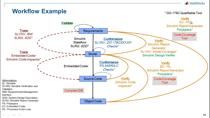
- Simulation of a high-level behavioral system model that serves as a golden reference for the hardware-software implementation on the RFSoC device and an elaborated implementation model for code generation
- Analysis of two alternative ways to perform hardware/software partitioning of the range-Doppler algorithm, using simulation and on-device profiling to determine the latency and implementation complexity
About the Presenter
Tom Mealey is a Senior Application Engineer at MathWorks. He supports customers in adopting Model-Based Design to accelerate the design and deployment of complex control and algorithmic applications including communications, radar, computer vision, audio, and deep learning. He is an expert on the design and implementation of applications targeting the Xilinx Zynq platform and other SoC devices. Prior to working at MathWorks, Tom worked at the Air Force Research Laboratory’s Sensors Directorate, where he was involved in projects implementing digital signal processing on FPGAs and SoCs. Tom earned his B.S. in Computer Engineering from the University of Notre Dame and his M.S. in Electrical Engineering from the University of Dayton.
Recorded: 29 Jul 2021
Hello, everybody. Welcome to this webinar, Performing Hardware/Software Co-design for Xilinx RFSoCs Gen3 Devices using MATLAB and Simulink. My name is Tom Mealey, and I'm an application engineer here at MathWorks on the HGL and SOC team.
Brief agenda. What we're going to cover today. We'll talk first about the RFSoC device, provide an overview. We'll talk about the hardware/software co-design methodology we can use to design applications for RFSoC.
We'll talk about a target application for RFSoC, Range-Doppler Radar. And then we'll go through the design methodology to create that Range-Doppler Radar system.
All right. First, I'd like to start with a demo and hardware here for Range-Doppler Radar. So this is running here on my GCU 216 board Gen3 RFSoC evaluation board. So what I'm going to show is a radar target simulator running on the FPGA, which is sending out four channels of data to the decks, looping that back to four ADC channels, and then doing Range-Doppler processing to estimate the range of velocity of our simulated targets, OK.
So let's take a look at that running. So this script here, which is going to go out and start the application running on the hardware. And so what we're looking at here on the left is the Range-Doppler response which is being computed on the RFSoC device between the FPGA and processor.
So we can see we have two targets here given by the peak and amplitude of these yellow dots. And then we feed that to a detector and pull out our estimated range of about 3,000 meters, 4,000 meters, and velocity about 100 meters per second and 150 meters per second.
All right. So this is a four-channel demo where I've incorporated beam-forming. OK, so we're simulating your a four-element uniform linear array front end in our radar target model. And so I'm going to steer now the angle, my beam former to 50 degrees azimuth. And I know this target is at 50 degrees azimuth.
And so what we're going to see is when we steer, now we only see this target. The other one is kind of faded into the noise, because we placed it into the null of our beam pattern, right, where for the other target now, we've increased the gain of the return from this target coming back to the antenna.
OK, so I want to steer it now to negative 47 degrees azimuth, which is where my other target is. OK, now we'll see this target disappear. And now we only see our target at about 3,000 meters. OK, and that's the fact of the, again, the beam former, where we're steering towards this target and nulling out the energy coming from the other direction or coming from this target. So now I can steer back to 0 degrees azimuth, and we'll see both targets appear.
All right. So let's stop this, and then back up, and take a look at how I created this system with MATLAB and Simulink. All right. So the high level question I want everyone to be thinking about as we go through the presentation here is, how can I make design decisions before touching the actual hardware?
So whether you're a hardware designer, embedded software engineer, or systems engineer who works with either of these folks, this is something you've likely thought about, right, because as much as we wish that the algorithm implementation would be agnostic of the target hardware, usually you're going to end up making design decisions based on the actual hardware you're targeting, right?
And so you have to be aware of the architecture of your system when you are going through your design and implementation. So ideally you want to make some of these decisions early on in the design process before you've gotten to the point where it's actually in hardware. So we're going to think about how we can do that with MATLAB and Simulink.
All right. Now let's talk briefly about the RFSoC device. So what it is, it is a System-on-Chip from Xilinx with integrated FPGA processor and RF ADCs and DACs. In the Gen3 devices-- the latest family-- provides up to 16 ADC and DAC channels, 5 and 10 giga samples per second, receive and transmit, and 6 gigahertz of direct RF bandwidth.
So really powerful converter front end in addition to very powerful processing capabilities. So you know why would you design your system based on our RFSoC as opposed to separate components. Well primarily, one, to reduce the power and size footprint of your system. You benefit also from simplified interfaces between all of the components, really the processing system, the programmable logic, and the converters.
And then finally, your development time can be shortened in large part because of these simplified interfaces. We see RFSoC used in a lot of applications-- you know, wireless communications, 5G and LTE, and aerospace and defense world, and things like radar, Adaptive beam forming, EW second, test and measurement, instrumentation, right?
And really the bottom line is that RFSoC is not a hobbyist part. It's not like an SDR type of, my first radio type of device, right? It's a big part for big applications. And so to be successful in designing applications for RFSoC, a design methodology that integrates the hardware, software, and RF components of the system level is crucial, OK.
So let's talk about hardware software code design, which is going to incorporate that these requirements, we just talked about for this design methodology. And so what defines hardware/software co-design is having a system level specification, which is used to inform the design and implementation of the hardware, software, and interface between hardware and software all kind of in tandem as opposed to having separate specifications and designs for each of these.
Some of the common challenges with hardware/software co-design and things like deciding how to partition your algorithm with what runs in the processor servers, the FPGA. How does the interface bandwidth affect system performance, how to identify processing bottlenecks new system, and then how the hardware software interface teams can all work together effectively, right?
And so especially this interface component is really crucial and often could be neglected, right? But to illustrate the importance of having a well-defined interface and kind of accounting for that along with your hardware and software in parallel, let's take a look at a very common paradigm with hardware/software co-design, which should be the FPGA streaming data to the processor.
And so you have some algorithm operating on a period on the order of nanoseconds, processing samples of data, feeding that into a buffer, and then another part of your algorithm, running in software-- let's say an ARM processor, processing that data from the FPGA in chunks or frames at a frame rate on the order of something like milliseconds.
So one way to model that interface between FPGA and ARM is just a basic buffer, rate change, right? When you get enough samples from the FPGA, then they just execute with that data on the ARM.
But if you think about what's going on under the hood, it's a little more complex than that. So the way that this buffer is implemented usually is with a shared DUR memory. So along with that, the way it's implemented between your FPGA algorithm and the memory controller, you're going to have to have a FIFO because they're operating at different rates.
So determining what's an appropriate rate you can write to that FIFO without overflowing it based on the burst rate of the memory controller and the bandwidth there.
On the processor side, the actual memory read operation is usually not completely periodic. It's more interrupt-driven or asynchronous, and so, you have a memory reader like a device driver, which drives the feeding the data to your algorithm on the processor. So how do you synchronize the software with the memory reader?
And then you have usually within memory a managed ring of buffers accomplished through usually a DMA engine. And so how do you allocate? Make sure you have enough space allocated in memory, so that your ring of buffers is not overflowing.
Now within the context of a system, oftentimes you can have other memory readers and writers contending for access to this DDR. On the processing side, within the operating system context, often you have other threads and processes that want processor time.
And then along with that, we see we have a number of parameters that we need to determine. Things like the birth size, number of buffers, how do you synchronize? Things we just talked about. And so, how can you account for all of these parameters of your interface early on in the design process before you actually get the hardware?
So a tool that we have in Simulink to do exactly that. It's called SoC Blockset. And so what you can do with SoC Blockset is accomplish this system level design that we talked about. Hardware, software, and interface through modeling and simulation early on in the design process.
Make those performance analysis and design trade-offs based on simulation before you get to the implementation and later on in the design process.
So SoC Blockset provides a number of simulation capabilities related to this, as well as on-device profiling that you could use to characterize the actual performance of hardware and verify that against your simulation. In SoC Blockset, the framework integrates well with MathWorks's other co-generation tools, for HGL and C-Code. So that you can generate code directly from your simulation model and automatically deploy to target hardware. You're using the model-based design approach.
So some of the boards that are supported by SoC Blockset out of the box include some common Zynq and Intel SoC seaboards, including now in 21A. The ZCU216 gen three RFSoC kit, which I was showing before. And so you could select one of these supported boards that come with our hardware support package, or register your own board, as well.
So let's take a look now at our target application that we saw earlier, Range Doppler Radar. And so just to review, a Range Doppler Radar system is a pulsed radar that the goal is to estimate range and velocity of target objects.
And so let's just start with some system specifications here. We have 200 megahertz of signal bandwidth send it to x-band. We have a four element uniform linear array antenna frontend where we need to perform beam forming on receive. We need to estimate up to five kilometers of max range for our targets per pulse interval, and then we must integrate 512 pulses max per coherent processing interval, which is going to determine the resolution of our velocity processing.
Now, before we get into this design process, we'll put on our systems engineering hat for a second, and some of the questions we're going to be thinking about as we go through this would be what does the algorithm look like, first of all?
To produce the range of velocity estimates, what type of processing is performed? What are the data rates from the converters through the FPGA to software? What's the rate and bandwidth of my data? When we get into partitioning, what should be implemented in the programmable logic or FPGA versus what should be implemented in software? And as we think about the different partitioning options, which approach is going to have the best throughput?
Of course, ultimately, performance going to be a big consideration, but also, what approach will be the simplest to implement? Time can be a big concern for these projects, and so oftentimes, we may want to choose an approach that is going to be safer or simpler. So let's jump in now to the design methodology to create this Range Doppler Radar system using workflow based on MATLAB and Simulink.
So first, we'll start here with the system-level specification, and for any RFSoC-based application, the very important first step is to perform some frequency planning. So based on our system specs, we know there's signals at x-band, about 10 gigahertz. But the RFSoC max input frequency or bandwidth is six gigahertz RF.
So how do we go from RF to digital baseband and vise versa? That's going to involve selecting a number of parameters here, including the intermediate frequency or IF, the sampling rate that converters run at, the frequency of the built-in NCL mixer, the decimation interpolation factors, and then finally the FPGA clock rate.
So I'm showing here a diagram from the product guide from Xilinx for the RF data converter, which shows the digital down conversion chain built into the RFSoC device. So from left to right, we have our RF signal coming in, an analog signal, with some RF frequency. Less than six gigahertz.
We can sample that up to 2.5 giga samples per second with the 16 channel variant of the gen three RFSoC devices. If it were eight channel, we could get up to five giga samples per second. Then we have a complex mixer, where we can mix the signal down to baseband. And then INQ decimators, where we can select between one and 40x decimation. And then from there, we can further reduce the clock frequency of the FPGA by packing between one and eight samples per clock cycle.
So let's start by choosing a decimation factor based on the signal bandwidth. One way to approach this is as we think about it. We have a 200 megahertz signal bandwidth, and from the RF data converter product guide, we can read that decimation filters have an 80% Nyquist pass band. So with that, we can create this little inequality.
Let's say choose a decimation factor of eight and plug that in. So that gives us that we need to sample our ADCs at a rate greater than or equal to 2 gigahertz, 2000 megahertz. So our effective sampling rate is going to be 2 gigahertz divided by the decimation rate of eight or 250 mega samples per second.
But then we can further reduce that rate by packing two samples per FPGA clock, or stream clock, so that we only need to clock our logic at 125 megahertz. And so that's going to make it a little easier to meet timing. Your FPGA person will thank you.
So now, we choose an IF of 2.5 gigahertz. Remember, we're sampling at 2 gigahertz, and so what happens is the signal alias is down from the third Nyquist zone now to be centered at 500 megahertz. And then from there, we can choose our NCO frequency to be negative 500 megahertz, so that the signal shifts down to be sent to baseband.
And so we can simulate that whole process with Simulink. So here, I have a model that I built up of the RF data converter digital down conversion chain. And so we're simulating our signal coming in at IF, going through the ADC, getting sampled, being mixed with the complex mixer and then going through 8x decimation or three stages of 2x decimation is how it is implemented.
So we can plot here the spectrum. Here's our IF signal centered at 500 megahertz like we expected. And then you look at the baseband spectrum after the down conversion, and we see here that spans from negative 100 megahertz to positive 100 megahertz. There's our 200 megahertz of bandwidth, and that verifies that our signal ends up in the right spot. It gets mixed down like we'd expect it to.
So once we are comfortable with our frequency planning, we can build up a system-level model. So it should say a high-level behavioral system model, where the keyword is behavioral. We're not thinking about the hardware-oriented implementation stuff. Really, we just want to get the system-level behavior figured out, make sure that all of our system-level specs are in order. And this will serve as a reference for our actual hardware and software implementation later on that we can compare.
Numerically, does our implementation version match this high-level behavioral system model? So let's take a look at this model. Right here, we're simulating the RF domain, which is the waveform. And then the radar target environment or model, as well as the digital signal processing. Which produces the Range Doppler Map and the detections.
And so after we complete one CPI, now we see we have this one target showing up. We're incorporating beam forming like we saw in the hardware demo. So even though there are two targets in the environment we're beam forming, and we only see one. So we see that show up here on the Range Doppler Response, as well as the detection map output.
And so just to dig into the guts of this model a little bit, so we have our waveform defined. Just an LFM or linear FM pulse waveform. And this goes into this radar target model, which is a model reference. Which you're not familiar with that. Not a Simulink user. This is a separate Simulink model, which I can pull into and use it in multiple top-level Simulink models. So a really useful way to componentize your model.
But this radar target model here, these are blocks mostly from the phased array system toolbox. So I'm simulating the path from the transmitter through this free space channel out to two different targets, and then the returns back from the targets to the receiver.
And so under the hood and the receiver, I'm modeling my receive array, which is the uniform linear ray. Which gives me the four channels of output. And here, then I feed that to a beam former. So we have our four antenna channels coming in. We form one beam channel out. Then we do our Range Doppler processing.
So in here, we're doing some range gating or ignoring the first length of samples coming back per pulse interval. We buffer up multiple pulse intervals and then form this matrix, which we feed to Range Doppler Response. So that's outputting this view you see here. And then the Range Doppler Response or map, we feed into this 2D CFR detector. We can visually see here. Here's a target, but mathematically, the CFR is going to tell us hey, there's one target right here.
So again, this is a really useful first step in just simulating the behavior of our radar system. And not only in the RF domain or the radar scene but including the signal processing, as well.
Now that we've modeled our system at a high level, we can start thinking about how to partition it between hardware and software. So the first very crucial step in this process is to elaborate the high-level components in your algorithm. So what that means is you're looking at what's going on under the hood and decomposing high-level blocks into their underlying operations where you can understand the things like data sizes and types.
So for example, the Range Doppler Processing block, we saw that was just a block in Simulink in my system model. But ultimately, we need to understand what's going on under the hood? What is it doing to produce that Range Doppler map? So this elaboration of high-level functions is the first step that we need to do to partition the algorithm effectively.
So the approach that I suggest to take is to re-implement the high-level block in parallel with the original, so that you can compare the outputs easily. And so that's exactly what I did, so you can see at the top level, my model looks pretty similar to the previous one. I have my waveform, target model, beam former, all the way into this Range Doppler response.
But now I'm implementing this Range Doppler response in MATLAB code in parallel. So you can see when I just break this down, it's really pretty simple. The important parts are a filter along one dimension, and then an FFT along the other dimension. So these filter and FFT. Now we're getting into really basic foundational blocks in DSP systems.
And so I've implemented that in MATLAB code in a way where I can really easily understand what these fundamental blocks are. And then in Simulink, I feed these to some signal comparison and then an assertion, so that I can simulate them together and verify that I'm-- What I'm doing under the hood, I know exactly what that is. I know how to get the exact same output as this high-level block. So just verifying that your elaborated version matches the original, high-level version.
So going through the elaboration step now allows us to perform some analysis on the characteristics of the algorithm and the pattern of the data flowing into it. So we know that we have range samples coming in for an individual pulse linearly in time, and we collect that range data over multiple pulse intervals to form up a matrix of data.
So along the range dimension, we are computing a matched filter or FIR filter, and what we can learn here is that the range computation could be performed immediately as the data streams in from the ADC or really from the output of the beam former.
Whereas for the FFT, which is performed along the other dimension of the matrix, we need to have the entire matrix or frame present before we do that computation because it's along the other dimension.
So now when we go into partitioning our system or the algorithm from end to end. So we'll say for the beam former, that makes sense to just put it on the FPGA. It's directly from the ADC data into a phase shift being formed, which is really simple. It's just a complex multiply. It makes sense to keep that on the FPGA based on the signal path or the data path.
Detection, on the other hand, we'll put that on the ARM processor because usually, your detection is going to be feeding information to some other high-level functions or processes. Like things like a cluster, a tracker. So it makes sense to have that part close to these other high-level components.
But now for the Range Doppler processing, or the matched filter in FFT, we need to decide do we put these on the FPGA or the ARM?
So let's lay out two possible options of this partitioning. So in one scenario or option A, we have the matched filter and FFT both on the FPGA. In option B, we have the matched filter on the FPGA but the FFT on the ARM processor. And so, what we need to decide essentially now is to compare these two approaches. Should we do the FFT on the ARM or the FPGA?
So let's think about option A, which is the FPGA-based FFT. So the first thing we think about here is the size of our data matrix because we have to have the entire matrix present before we can do the computation. And so, we have up to 4,096 by 512 samples with 14 bits of ADC sample times 2 for IQ. And that gives us 56 megabits of data that we need to store.
And so, we might think can we just store that in block RAM on the device? That would be really simple. We look at the product table for the ZU49DR device, and unfortunately, we only have 38 megabits of block RAM available. So that's going to be too large, and what that means is we have to store it in external DDR.
And so, based on the order that the data comes in, we're going to write to DDR in order after the matched filter and then read it from DDR in a transposed order for the FFT.
And so, we can estimate the timing of this DDR transpose using blocks and Simulink. So what we're going to find is that the in order write operation to DDR is going to be fast, while the transposed read is slow and inefficient. So let's take a look at this model.
So this is really simple. It's built to use in three blocks. This right traffic generator, which emulates the right pattern of the in order data after the matched filter being written to memory. And then the read traffic generator emulates the transposed read operation where we're reading the data in the order that we need for the FFT.
And so after we run simulation, look at the memory controller block. So the memory controller now is what we're using to simulate the behavior of the interface to DDR, so that's what these traffic generators are talking to.
So the first thing I want to point out is that we see here that the hardware board is displayed. So what that means is for all of the supported boards, SoC Blockset that we've characterized the performance or behavior of the memory controller on that board. So you can see here all of these behavioral parameters are already populated based on the characterization of this board.
And so now under the performance tab, we can look at the bandwidth of the read and write traffic, and so what we're going to see here is that the write operation achieves really high bandwidth, 500 megabytes per second. Whereas the read operation, we only get about 25 megabytes per second.
And we're writing and reading the same amount of data, but the read is going to be inefficient because the data is not stored contiguously in memory in the way that we need to access it. We need to read one word at a time versus the write. We can just put it all in order and use high-burst lengths, which is going to be more efficient from a protocol standpoint.
So with that behavioral model, we can plug-in the time estimate for our full max frame here, 4,096 by 512. It's going to be 438 milliseconds, and that's our estimate of doing just the transposed memory.
So now for option B. So we have our 512 by 4,096 matrix. The way that the dimensions that we're competing along here are such that we perform at 512 length FFT 4,096 times. But each of these FFT computations can be performed in parallel, and so we could take advantage of the fact that we have a quad core ARM Cortex A53 processor and distribute the work between the four cores for a four times speed-up.
And so to analyze the timing there, we can just measure the actual timing and hardware using profiling tools and Simulink. So we're going to use something called processor in the loop to measure the actual timing of the velocity process being done in software.
So I have this model here where I'm defining some test input, and this is just random data that I'm plugging in. You see I have a 1,024 by 512 matrix. This is just one fourth, 25% of the chunk of the overall matrix, which is going to be computed up. And what we're doing is, for this underlying model here, which contains an FFT block, we're generating C-Code which is target optimized for the ARM processor. So that it'll take advantage of neon floating point instructions.
And we're measuring how long that takes to execute that FFT on the hardware.
That will pop up with this profiling report.
So the FFT takes up most of the time here, about 372 milliseconds, but we have to do, also, a matrix transpose and data type conversion. And so, the total execution time, on average, for this step is about 476 milliseconds. Again, this is all real data that we just measured in hardware. And so, now we have this number that we can use to compare with the previous approach or option A.
So laying them out, we saw that our estimate for the bottleneck here for the FFT on the FPGA of that memory transpose, we estimate the latency about 438 milliseconds. Whereas for option B, the software FFT, we measured a 476 millisecond execution time.
So just based on that factor, option A is superior, but as we talked about before, latency is not always the only factor to consider. So option A is going to bring some high amount of complexity in terms of the implementation just by its nature being implemented on the FPGA. And having to write a memory interface logic to do that transposed read operation versus the software-based FFT.
I just dropped a block into my Simulink model that already generates target-optimized code. It's really simple to implement, and latency is not-- You're not going to take that much of latency hit, so in this case, we're going to start with option B due to its simpler implementation.
So now that we've decided on a partitioning scheme, we're going to move into the first phase of our design implementation where we integrate the hardware, software, and their interface all in parallel in one Simulink model.
And so I've got this model here, and you can see here at a high level, I have things partitioned out into the domains that they're going to be executing in. The FPGA, the processor. So I still have this radar target model under the hood. This is the same model that I've been using throughout the process, and I also have this memory channel, which includes that DMA or buffer between the FPGA and processor. So this is how we stream the output of the matched filter to the processor.
And so I've already run a simulation, but some of the things we can see here. So let's take a look under the hood here in the processor model. So we used this Task Manager block and defined the partitioning of our software. Let me bring this guy up.
So let's plot this out and simulate data inspectors. Now we can plot the execution of our software tasks in simulation, so I've already run simulation for this model. I can plot now the execution of my four different tasks. So the four FFT processing tasks, so I have my core zero task, core one task, core two task, core three. So not super interesting. They all do the same thing, so naturally, they're all executing at the same time in parallel processing those individual chunks of the overall matrix.
But then we also can plot here. There's a fifth task, which is the DMA reader. So we can see that execute for a short amount of time. This reads the data from the FPGA before handing it off to the four processing tasks to run in parallel. So we can plot the execution of all that through simulation, and more importantly, include the latency of the software in our overall system performance and simulation timing.
On the FPGA side, so we have the now really high-level version of our processing. You can see I still have matrix signals. Ultimately, I'm not going to generate code from this, but I can still include the timing of the FPGA and model the rate at which this data is executing. So I can include here's my beam former, range gating, matched filter, all on the FPGA.
Then my interface to the DMA channel, which is then being read by the processor. So here's a DMA reader feeding these four tasks in parallel to do the FFT processing.
So the last step here. So after we've built up a system model which includes our hardware software partitioning. Now, we're moving into the prototype stage, which is what I showed before. So again, here's the high-level overview of that system where we partitioned out not only the range of velocity processing between FPGA and software, but added some extra details here.
Now for my prototype system, we have the target simulator, where I'm storing the pre-computed target environment data and transmitting that out of the deck. And then I also have a command interface on the software side, which is used to coordinate the timing and execution of all of this.
So let's take a look at the model that I built up to generate code for this demo. So compared with the previous iteration in the model, we can see there's a lot more detail that's been added here. So we had before, our DMA channel from the FPGA to the processor. The output of the matched filter being sent to the FFT computation.
We've added another memory channel here, which is used by the processor to send data to a lookup table on the FPGA. Which is, in this case, the radar target simulation data. So we can change our radar or our test scenario dynamically by writing the data to the FPGA from the processor.
So we also have in our simulation model, the interface between the host PC, which is what I showed just my MATLAB terminal. Which is sending UDP packets to the process on the target, so we're simulating all that behavior. And then, we've also added this RF data converter block, which is going to provide the digital interface from the FPGA to the actual converters on the device.
So we've broken all this out here with the AXI stream signals, the data invalids. And this is what will generate HGL code to interface with this RF data converter IP.
And so just to show you the level of detail here in our final version of the model. So on the FPGA side, dig into say, the range processing, for example. We're doing a filter, but here, I'm really getting into a very detailed architectural implementation. Where we're doing a two sample vector FIR with complex coefficients and complex inputs.
So I partition that out. Under the hood, these use filter blocks that generate code, but I partitioned out, so that we could do the two samples per clock cycle. And then on the software side, for example, show this command and control function. So this is a separate thread here which just handles UDP packets from the host.
So this is all implemented in a MATLAB function block, so I take a packet of UDP data in, parse a command data structure, and then use that to determine mostly what data to write to registers on the FPGA. So here's a number of parameters that we can set dynamically at runtime through the AXI light slave interface on the FPGA IP core. We're writing from software.
And so I can generate code for this whole model all using this SoC builder workflow, and so just go and launch this. But we can see here we have our models partitioned out. Here's the FPGA model and the processor model, and so you're telling the tool which parts of the model you're going to generate HGL code to target the FPGA and which parts are going to target the processor and generate C-Code. So this wizard, you can use to go through the whole code generation and deployment process.
So we've reached the end of our time here, but if you liked what you saw, if you're interested in trying some of this yourself, here are all the products that I used to build this demo. You can check out MathWorks.com/RFSoC to learn more details about the different tools that MathWorks offers to support RFSoC development workflows.
And then finally, contact your MathWorks account manager. For more information, get in touch with one of our application engineers. We'd be happy to hear more about what you're doing and guide you in getting started with these workflows. Thanks for your time, and I hope to hear from some of you soon.