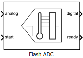
Flash ADC
N-bit ADC with flash architecture
Libraries:
Mixed-Signal Blockset /
ADC /
Architectures
Description
An N-bit flash ADC comprises of a resistive ladder that contains 2N resistors and 2N-1 comparators.
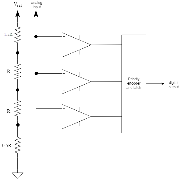
The reference voltage of each comparator is 1 least significant bit (LSB) higher than the
one below it in the ladder. As a result, all comparators below a certain point will have input
voltage greater than the reference voltage, and a logic 1 output. All
comparators above that point will have input voltage smaller than the reference voltage, and a
logic 0 output. The output of
2N-1 comparators are passed through a priority
encoder to produce the digital output. This encoding scheme is called thermometer
encoding.
Since the analog input is applied to all the comparators at once, the flash ADC architecture is very fast. But the ADC has low resolution and high power requirements due to a large number of resistors required to implement the architecture.
Ports
Input
Analog input signal, specified as a scalar.
Data Types: double
External clock to start conversion, specified as a scalar. The analog to digital conversion process starts at the rising edge of the signal at the start port.
Data Types: double
Output
Converted digital output signal, returned as scalar.
Data Types: fixed point | single | double | int8 | int16 | int32 | uint8 | uint16 | uint32 | Boolean
Determines whether the analog to digital conversion is complete, returned as a scalar.
Data Types: double
Parameters
Configuration
Number of physical output bits, specified as a unitless positive real integer in the
range [1, 26]. Number of bits determines the
resolution of the ADC.
Programmatic Use
Use
get_param(gcb,'NBits')to view the current Number of bits.Use
set_param(gcb,'NBits',value)to set Number of bits to a specific value.
Data Types: double
ADC dynamic range, specified as a 2-element row vector in volts.
Programmatic Use
Block parameter:
InputRange |
| Type: character vector |
| Values: 2-element row vector |
Default:
[-1 1] |
Data Types: double
Select to connect to an external start conversion clock. By default, this option is selected. If you deselect this option, a Sampling Clock Source block inside the Flash ADC is used to generate the start conversion clock.
Frequency of internal start conversion clock, specified as a positive real scalar in hertz. Conversion start frequency (Hz) determines the rate of the ADC.
Dependencies
This parameter is only available when Use external start clock is not selected.
Programmatic Use
Use
get_param(gcb,'StartFreq')to view the current value of Conversion start frequency (Hz).Use
set_param(gcb,'StartFreq',value)to set Conversion start frequency (Hz) to a specific value.
Data Types: double
RMS aperture jitter added as an impairment to the start conversion clock, specified as a real nonnegative scalar in seconds. Set RMS aperture jitter value to zero if you want a clean clock signal.
Dependencies
This parameter is only available when Use external start clock is not selected.
Programmatic Use
Use
get_param(gcb,'StartClkJitter')to view the current value of RMS aperture jitter (s).Use
set_param(gcb,'StartClkJitter',value)to set RMS aperture jitter (s) to a specific value.
Data Types: double
Clock edge type that triggers the output update:
Rising edge— the output is updated with the rising edge of the clock signal.Falling edge— the output is updated with the falling edge of the clock signal.Either edge— the output is updated with both the rising and the falling edge of the clock signal.
Programmatic Use
Use
get_param(gcb,'Trigger')to view the current Edge trigger type.Use
set_param(gcb,'Trigger',value)to set Edge trigger type to a specific value.
Inherit the output polarity and data type from the analog input signal to the ADC. If you select this option, the ADC ignores the Output polarity and Output data type parameters. The ADC output has the same polarity as the input and the data type is double.
Defines the ADC output data polarity.
If Output polarity is set to Auto, the
minimum and maximum values of the output are determined by the polarity of the
Input range.
If Output polarity is set to Bipolar,
the outputs are between -2Nbits-1 and
2Nbits-1-1.
If Output polarity is set to Unipolar,
the outputs are between 0 and
2Nbits-1.
Dependencies
To enable this parameter, deselect the Match input scale option.
Programmatic Use
Block parameter:
OutputPolarity |
| Type: character vector |
Values:
Auto | Bipolar |
Unipolar |
Default:
Auto |
Defines ADC output data type.
Unsigned integers and fixed-point types (fixdt(0,Nbits))
are not available when the Output polarity is set to
Bipolar or Auto.
Signed integers and fixed-point types (fixdt(1,Nbits)) are
not available when the Output polarity is set to
Unipolar.
Dependencies
To enable this parameter, deselect the Match input scale option.
Programmatic Use
Block parameter:
OutDataType |
| Type: character vector |
Values:
double | single |
int8 | int16 |
int32 | uint8 |
uint16 | uint32 |
fixdt(0,Nbits) |
fixdt(1,Nbits) | Inherit: Inherit
via back propagation |
Default:
fixdt(1,Nbits) |
Define how the Flash ADC block is used in the simulation. You can use the block as a Simulink® block, or use the System object™ implementation (either interpreted or code generation) for more control.
Impairments
Select to enable linearity impairments such as offset error and gain error in ADC simulation. By default, this option is deselected.
Shifts quantization steps by specific value, specified as a scalar in %FS, FS, or LSB.
Note
The full scale range of the converter is defined as the difference between the last and first code on the +0.5 LSB compensated transfer curve. In a +0.5 LSB compensated transfer curve, first code is 0.5 LSB wide while the last code is 1.5 LSB wide. The input values must be considered within the full scale range of the converter.
Note
LSB is calculated by the equation .
Dependencies
To enable this parameter, select Enable Linearity Impairments in the Impairments tab.
Programmatic Use
Block parameter:
OffsetError |
| Type: character vector |
| Values: real scalar |
Default:
3 LSB |
Data Types: double
Error on the slope of the straight line interpolating ADC transfer curve, specified as a real scalar in %FS, FS, or LSB.
Note
The full scale range of the converter is defined as the difference between the last and first code on the +0.5 LSB compensated transfer curve. In a +0.5 LSB compensated transfer curve, first code is 0.5 LSB wide while the last code is 1.5 LSB wide. The input values must be considered within the full scale range of the converter.
Note
LSB is calculated by the equation .
Dependencies
To enable this parameter, select Enable Linearity Impairments in the Impairments tab.
Programmatic Use
Block parameter:
GainError |
| Type: character vector |
| Values: real scalar |
Default:
2 LSB |
Data Types: double
Position of the failed comparators, specified as a row vector with positive real values.
Dependencies
This parameter is only available when Enable Linearity Impairments is selected.
Programmatic Use
Use
get_param(gcb,'Bubbles')to view the current Missing codes.Use
set_param(gcb,'Bubbles',value)to set Missing codes to a specific value.
Data Types: double
Select to enable timing impairments such as conversion delay in ADC simulation. By default, this option is deselected.
Latency of the analog to digital converter, specified as a nonnegative real scalar.
Dependencies
This parameter is only available when Enable Timing Impairments is selected. If you are using the Flash ADC in the System object mode, this value is rounded to the nearest multiple of the sample interval.
Programmatic Use
Block parameter:
ConversionDelay |
| Type: character vector |
| Values: real scalar |
Default:
0 |
Data Types: double
Select to enable increased buffer size during the simulation. By default, this option is deselected.
Dependencies
To enable this parameter, set Simulate using to
Simulink blocks in the Configuration tab and select
Enable Timing Impairments in the Impairments
tab.
Number of extra buffer filters available during simulation, specified as a positive real scalar.
Selecting different simulation solver or sampling strategies can change the number of input samples needed to produce an accurate output sample. Set the Buffer size to a large enough value so that the input buffer contains all the input samples required.
Dependencies
To enable this parameter, set Simulate using to
Simulink blocks in the Configuration tab. Then select
Enable Timing Impairments and Enable
Increased Buffer Size in the Impairments tab.
Version History
Introduced in R2019a
MATLAB Command
You clicked a link that corresponds to this MATLAB command:
Run the command by entering it in the MATLAB Command Window. Web browsers do not support MATLAB commands.
Select a Web Site
Choose a web site to get translated content where available and see local events and offers. Based on your location, we recommend that you select: .
You can also select a web site from the following list
How to Get Best Site Performance
Select the China site (in Chinese or English) for best site performance. Other MathWorks country sites are not optimized for visits from your location.
Americas
- América Latina (Español)
- Canada (English)
- United States (English)
Europe
- Belgium (English)
- Denmark (English)
- Deutschland (Deutsch)
- España (Español)
- Finland (English)
- France (Français)
- Ireland (English)
- Italia (Italiano)
- Luxembourg (English)
- Netherlands (English)
- Norway (English)
- Österreich (Deutsch)
- Portugal (English)
- Sweden (English)
- Switzerland
- United Kingdom (English)