Reuse of Simulink Components Within Chip-Level Design and Verification Environments
Simone Saracino, STMicroelectronics
Diego Alagna, STMicroelectronics
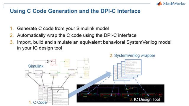
To keep pace with market needs for performance and cost efficiencies, the architecture of integrated circuits (ICs) needs to be highly optimized. Many semiconductor engineering teams are using Simulink® as their main tool to perform such optimizations, since it allows them to easily model and simulate multidomain systems, including analog and digital components. Moreover, this approach enables verification activities within Simulink, before the implementation phase has started, allowing engineers to find bugs early and shorten lead times. In this presentation, you will learn how Simulink design models and testbenches can be reused throughout the IC design cycle. We will demonstrate how design models can be converted to synthesizable RTL through HDL code generation and how Simulink verification components can be reused within UVM verification environments, avoiding duplication of effort between system-level activities (performed within Simulink) and RTL-level activities (performed using EDA tools).
Published: 30 May 2022
[MUSIC PLAYING]
Good morning, everybody. My name is Diego Alagna, and I work as the digital team leader in automotive group. We will talk about how to improve the system level verification and how to reduce the system level verification components in the test case within a chip-level design and verification environment.
Here is our agenda. We start with a quick introduction about why it is important to do verification at the system-level. Then we will talk about the system-level design model under analysis and how it has been verified-- in particular, how part of the verification has been shifted left, moving it from RTL to system-level.
We will then talk about how system-level test bench components and test cases have been reused within the chip level UVM test bench. After that, we will show how the system-level design model two has been reduced by generating RTL code from it. We will then finish by discussing the results and the planning of future announcement.
Here is the introduction. Semiconductor industry progress until now has been following the Moore's law that states that the number of transistors doubles every two years. The Moore's law, as you know, has been slowing down over the last decade.
Nevertheless, market requirements are getting more and more aggressive on performance, cost, and time to market. So how to deal with such a situation? In the past, single IC components were getting significantly more performance from one technology in order to the next one. And this raise in performance was one of the main contributors to the overall IC enhancements.
Now that performance is not scaling so much anymore with the physical technology, we needed to work more at the system-level, and each component has to be optimized according to the overall IC architecture, taking into account how it interacts with other components.
Our team is involved in IC developments for the automotive industry. Here, the signal transistors are not so shrunk, because in the same IC, we need to integrate also some power electronics supporting high voltages or high currents. And they are now part, for example, for the sensing circuit.
With our technology, we can target the traditional device for automotive application, but also the new trends for car electrification and vehicle digitalization. For these kind of devices, the architecture optimization is fundamental to reach the business needs with strong competition.
This basically means doing more simulation and verification at the system level. As we said, this allows to enhance the architecture optimization, and additionally, moving at the verification earlier, allow to find the bugs earlier, and shorten the bug lead time, which leads in the end to better quality/time-to-market trade-off.
Now, traditionally, the system-level verification requires additional resources and effort. In this presentation, we describe how to avoid having to spend this additional effort by reusing the system-level test bench components. In the verification scenarios within the chip-level test bench. So we do more verification at the system level. And with their use the system level verification component at RTL level. Now, I'll let Simone introduce the system-level design model.
Thank you, Diego. In this slide, you can see our integrated circuit design. It is a voltage measurement unit, which is able to measure voltage input and communicates to microcontrollers through I square C interface. Our device under test is only form by gray block, which is our sigma-delta I2C.
It is composed by both analog and digital domains. In particular, the analog part consists on input stage and the sigma delta modulator, while the digital part is formed by decimator and the filtering blocks. Then, the TOP_CHIP is also other analog blocks such as power supply unit.
In the digital domain, there are I square C interface and other logic such as reducer map or FSM. In this analogy, we only discuss about gray block. This block on the schematic is the device under test, and it has been modeled and verified at system-level using Simulink platform.
This modeling includes both analog and digital components. In particular, the analog blocks are modeled using real numbers in discrete-time domain with the high sample rate, while the digital ones are modeled in a fixed-point, bit-accurate and cycle-accurate way. And it uses an ideal voltage generator for voltage input. The rest of the IC block are not modeled in the system-level using Simulink platform, but they are implemented with ST standard circuit.
Let's talk about the system-level verification. In Simulink platform, the DUT is also verified in order to anticipate it's real implemented design availability. The system-level test bench is composed by stimuli and scoreboard blocks.
This slide shows the detail of stimuli block. There are four types of DUT input. Analog voltage input, configuration parameters-- for example, ADC enable average filter stored in the register back by using I square bus interface.
Digital [INAUDIBLE] for I2C error stored in the external NVM memory. And debug configuration stored in test mode register map using FPI bus interface. I remember that all bus interfaces and memories are not modeled in the system-level environment.
All these inputs are modeled, of course, on the effective for the analog voltage input that is a real number. ADC enable signal that is dynamic parameter. For the future improvement, the stimuli can be randomized.
The scoreboard is a verification component that allows the functionalities of a design. It is composed by sampler, which samples I2C conversion data. Check valid which monitors the data valid signal and discard the first pass.
Check range which compares sampled data with the correctness data range. And check assertion which evaluates data correctness when check valid is true using a threshold symbolic block. In particular, the assertion Simulink block is to assert simulation error during system-level verification on Simulink and to insert an assertion custom command for chip-level environment. In this case, it has been added in UVM error.
Now, let's talk about reuse of system-level verification IPs within the UVM test bench. UVM is a Universal Verification Methodology for IC verification. Main purpose is to standardize the classic SystemVerilog testbench in a modular, reusable, and scalable testbench structure.
You can see on the left the classic SystemVerilog testbench that is made coding via the stimuli and the monitor blocks. The scoreboard checks the expected value with respect to stimuli input. On the right, the UVM approach is standardized the monitor and driver classes to be simple reuse in the different environment.
The system-level verification test cases need to be rerun at the chip-level. To avoid duplication of effort, system-level testbench is being reused using Simulink UVM generation capability. Generate UVM test bench from Simulink system-level environment using UVM build MATLAB command. It generates an UVM test bench equivalent to the Simulink one.
Since the Simulink DUT doesn't correspond to full IC, it is necessary to connect the UVM components generated by Simulink within UVM at chip-level verification environmental. Here, it is just an overview of the UVM generated files by Simulink to be integrated in our chip-level test bench.
Simulink HDL verifier tool generates standalone UVM test bench environment. So in case DUT corresponded to full IC device, it is possible to use it without modification. Moreover, HDL verifier generates also the UVM behavioral run model for DUT. In our chip-level environment, it's ignored since we use RTL generation for digital block and Verilog models for analog ones.
It is worth noting that each Simulink test case corresponds to a single UVM sequence. And to generate a single sequence, we need to generate the full UVM test bench environment. So in order to give good chip-level verification coverage, it needs a lot of sequences to integrate in our chip level verification environment.
The digital chip-level test bench environment is composed by chip-level top instance TOP_CHIP and UVM test bench.
TOP_CHIP in test bench are connected by interfaces. Interfaces function is of driving and monitoring the TOP_CHIP pin out. UVM components generated from Simulink are the yellow blocks. And they are sequence that generates transaction of Simulink test case. mw_DUT_agent data drives transaction on the DUT interface.
It also monitors data from top chip through them DUT interface. It is classic and input monitor. The first one translates the output from chip-level top into sequence item. The second one sends DUT inputs to the scoreboard predictor in order to compute the expected data output.
Scoreboard that compares the chip-level output translated into sequence item by monitor to expected one translated by input monitor. DUT interface-- that is the interface is generated from Simulink. Only voltage input is being connected to TOP_CHIP. The rest of the signal are input/output of DUT.
Since these signals do not [INAUDIBLE] as input/output of TOP_CHIP, but they are internal signals. In order to integrate the generated UVM components-- the yellow blobs-- in our chip-level verification environment, it needs to do some manual modification.
This modification consists of adapting generating the files. Then, it needs to insert an interface decoder in order to give the output of DUT interface to generate an existing high level transaction. Then it has been use a trigger in order to synchronize the start of generated sequence with the starting time at the system-level.
Now, we move on reuse of system-level design model. Let's talk about the green part, which is development in Simulink, and it can be reused in the implemented design. We use the Simulink HDL coder to generate the RTL code of that green block.
The RTL is a designed structure which models a sequence digital circuit. And starting from this code, a synthesis tool is able to generate the real schematic. In this way, our model described on Simulink at the system-level can be used at the chip-level design. This is an example of a generated RTL code, where you could see, for example, the entity of the block and the signal assignments.
The advantages of this reusable approach are, first of all, avoiding human errors in converting Simulink models to RTL. Then ensuring alignment between Simulink and RTL simulation. Then another advantage is fixing bugs at system-level model on the Simulink platform. And finally, the improvement workflow efficiency.
Let's now talk about the results. RTL verification time is being cut in half thanks to the reuse of Simulink collaterals. We avoided duplication of effort between system-level and the RTL-level verification. And we also saved RTL coding time by generating RTL from the Simulink design model, thus reducing the chance of human errors. And we finally ended up with a single source of test cases and design models with associated advantages.
Here are some future announcements. How to further improve the presented workflow? First, we want to simplify the integration of generated UVM component that we did the chip-level environment. Especially the way of interfacing generating components with chip-level drivers is to be reviewed.
Then we need to find an efficient way to manage the test cases. They are currently run sequentially one after the other. We have two ways to improve this. The first one is to have multiple Simulink test benches, each of them generating active cases.
And the second one is to use Simulink parameterization capability to allow the testbench components to generate different scenario. And another way not listed here is to use a mixture of these two approaches. Last, but not least, I want to introduce randomization. Here too, we have the two options to do this in Simulink using MATLAB and Simulink randomization engines, or to introduce it after UVM generation.
Here are our conclusions. In order to enhance the way we optimize the IC architecture, as discussed, we need to shift left part of the verification and move it to system-level. In this presentation, we have shown that removing verification to system-level doesn't necessarily mean more effort since as we described, system-level verification IPs can be reused at RTL-level. And that we can avoid duplication of effort even more by generating RTL from the system-level design model.
On top of that, this workflow allows to detect bug early at system-level before going to RTL, reducing the bug lead time. Thank you very much for your attention.